
Gerber File Ultimate Guide for PCB Manufacturing

Gerber Files Complete Guide
If you are preparing a PCB for fabrication, the Gerber package is one of the most important files you will send to the manufacturer. Many projects are delayed not because the circuit is wrong, but because the exported data is incomplete, the drill file is missing, the board outline is unclear, or the released files do not match the latest design revision.
A clean Gerber package helps the factory review the job faster, quote more accurately, and move the board into PCB manufacturing with fewer questions. It also reduces the risk of fabrication errors before the project reaches PCB fabrication and later production stages.
This guide explains what a Gerber file is, what a complete Gerber package should include, what a typical Gerber file example looks like, how to generate the files correctly, how to review them before submission, and what else may be required if the project continues into PCB assembly.
What Is a Gerber File
A Gerber file is the standard manufacturing output used to describe PCB layer data for production. It tells the factory how to build the board by defining copper patterns, solder mask openings, silkscreen markings, paste layers, mechanical outline, and drill locations.
It is important to understand that a Gerber file is not the same as the editable source used in PCB design. The design file belongs to the CAD environment, while the Gerber output is the manufacturing-ready release generated from that design. This is why board houses usually ask for Gerber files instead of native project files.
In real production, there is usually not just one Gerber file. A standard release contains multiple files, each representing a specific board layer or manufacturing function.
What a Complete Gerber Package Should Include

A complete Gerber package should contain everything the manufacturer needs to fabricate the bare PCB correctly. For most boards, that includes:
- top copper layer
- bottom copper layer
- inner copper layers for multilayer boards
- top solder mask
- bottom solder mask
- top silkscreen
- bottom silkscreen
- top paste layer if required
- bottom paste layer if required
- board outline or mechanical layer
- drill file for plated and non-plated holes
- routing or milling data when needed
If the design includes slots, edge plating, castellated holes, countersinks, unusual cutouts, impedance notes, or panel routing requirements, those details should also be included clearly. Missing one critical layer can stop the order before production starts.
If you want to compare Gerber with other release methods, this topic also relates closely to PCB file formats and the broader release package used in PCB design files.
Gerber File Example and Common File Extensions
Many people searching for a Gerber file example do not want raw code. They want to know what a normal manufacturing package looks like. A typical two-layer PCB release may include files such as:
- board.gtl for top copper
- board.gbl for bottom copper
- board.gts for top solder mask
- board.gbs for bottom solder mask
- board.gto for top silkscreen
- board.gbo for bottom silkscreen
- board.gko or board.gm1 for board outline
- board.drl or board.txt for drill data
You may also see the generic .gbr extension, especially when the software names all exported layers in a similar way. The exact extension can vary by CAD tool, but the important point is that every file is clearly tied to the correct layer.
For most modern workflows, RS-274X is the common Gerber standard because it carries complete layer image data and aperture definitions in a more practical way than older formats.
How to Create Gerber Files Correctly
Creating Gerber files is usually simple, but many mistakes happen during export. The most common issues are missing drill files, wrong layer selection, inconsistent units, and partial re-export after design changes.
A practical process looks like this:
- Finalize the PCB layout before export.
- Check pad geometry, copper pours, vias, outline, and special features.
- Export all required fabrication layers, not just copper.
- Generate drill data separately if the CAD tool requires it.
- Review the package in a Gerber viewer.
- Put the final release into one ZIP archive.
- Add notes for anything that cannot be understood from the layers alone.
Most mainstream design tools can generate Gerber files correctly, including KiCad. The software itself is only part of the process. Correct export settings and careful review matter just as much.
How to Review Gerber Files Before Sending Them Out
One of the easiest ways to prevent manufacturing delays is to open the exported package and verify it before submission. A quick review often catches the problems that later create expensive email exchanges or rework.
Before sending the files, confirm that:
- all required layers are present
- the board outline is correct
- drill holes align with pads
- solder mask openings expose the right pads
- silkscreen does not print over exposed copper
- inner layers are included if the board is multilayer
- cutouts and slots appear where expected
- the full package belongs to one final revision
This step is especially important when the project has gone through late layout changes. A common mistake is regenerating the copper layers but forgetting to regenerate the drill file or board outline.
Common Gerber File Problems That Delay Production
Even when the package looks complete, a few common issues can still slow the job down:
- missing drill data
- wrong outline layer
- mixed file revisions
- incomplete solder mask output
- unclear mechanical layer naming
- special fabrication requirements not documented
These problems affect more than fabrication accuracy. They also slow quoting, engineering review, and planning. If the factory has to ask whether a slot is plated, whether the latest outline is final, or whether panelization is required, the schedule moves immediately.
For companies trying to shorten lead time, this is why Gerber release quality matters almost as much as the layout itself.
What to Send Along With Gerber Files
For bare board fabrication, Gerber files and drill data are the core manufacturing outputs. But many projects need more than that. Depending on the board and supplier, you may also need to send:
- stackup information
- material requirements
- copper thickness
- surface finish requirements
- panelization instructions
- fabrication notes for special features
If the project will continue into assembly, Gerber files alone are not enough. The manufacturer may also need a BOM, pick and place data, assembly drawing, and any special handling or test notes. In practical sourcing and production workflows, this often connects directly with components sourcing and more coordinated turnkey PCB assembly.
Why Good Gerber Files Save Time and Reduce Risk
Well-prepared Gerber files help both the customer and the manufacturer. They make engineering review faster, reduce clarification emails, lower the chance of fabrication mistakes, and improve schedule predictability.
For the factory, a clean package makes it easier to understand the board and move it into production. For the customer, it creates a smoother path from release to finished PCB.
If you want fewer questions, faster turnaround, and more reliable results, the most effective place to start is with a complete Gerber package that has been checked carefully before submission.
In many real PCB projects, the difference between a smooth order and a frustrating one is not the complexity of the board. It is the quality of the manufacturing files sent at the start.
Different Extensions for Gerber Files
Gerber files can have various extensions depending on the type of data they contain. Here are some common Gerber file extensions and their descriptions:
- .gbr or .ger: These are the most common extensions used for Gerber files and contain information about different PCB layers, including copper traces, drill holes, and silkscreen layers.
- .pho: This extension is sometimes used for photoplotter output files, similar to Gerber files, containing the same type of information.
- .top and .bot: These extensions differentiate between the top and bottom layers of a PCB design.
- .smt and .smb: These extensions indicate the solder mask top and solder mask bottom layers of a PCB design, respectively.
- .cmp: This extension is sometimes used for the top layer of a PCB design that shows the components.
- .plc: This extension is sometimes used for the top layer of a PCB design that shows the placement of components.
- .sol: This extension is sometimes used for the bottom layer of a PCB design that shows the copper traces.
- .stc: This extension is sometimes used for the top layer of a PCB design that shows solder stencil information for stencil printing.
- .sts: This extension is sometimes used for the bottom layer of a PCB design that shows solder stencil information for stencil printing.
- .drd: This extension indicates drill data for a PCB design, showing where the holes should be drilled.
- .dri: This extension is sometimes used for the drill data for a PCB design.
Understanding these extensions helps designers and manufacturers identify the specific information contained in each Gerber file and streamline the PCB fabrication process.
Gerber File Extention from Different Software
| CAD Software | Gerber File Extensions | Probable PCB Layer Type |
|---|---|---|
| KiCAD | board-F_Cu.gbr | Top Copper Layer |
| board-F.Cu.gbr | Top Copper Layer | |
| board-F.Cu.gtl | Top Copper Layer | |
| board-F_Mask.gbr | Top Soldermask | |
| board-F.Mask.gbr | Top Soldermask | |
| board-F.Mask.gts | Top Soldermask | |
| board-F_SilkS.gbr | Top Silkscreen | |
| board-F.SilkS.gbr | Top Silkscreen | |
| board-F.SilkS.gto | Top Silkscreen | |
| board-F_Paste.gbr | Top Solderpaste | |
| board-F.Paste.gbr | Top Solderpaste | |
| board-F.Paste.gtp | Top Solderpaste | |
| board-B_Cu.gbr | Bottom Copper Layer | |
| board-B.Cu.gbr | Bottom Copper Layer | |
| board-B_Mask.gbr | Bottom Soldermask | |
| board-B.Mask.gbr | Bottom Soldermask | |
| board-B.Mask.gbs | Bottom Soldermask | |
| board-B_SilkS.gbr | Bottom Silkscreen | |
| board-B.SilkS.gbr | Bottom Silkscreen | |
| board-B.SilkS.gbo | Bottom Silkscreen | |
| board-B_Paste.gbr | Bottom Solderpaste | |
| board-B.Paste.gbr | Bottom Solderpaste | |
| board-B.Paste.gbp | Bottom Solderpaste | |
| board-In1_Cu.gbr | Inner Copper Layer | |
| board-Inner1.Cu.gbr | Inner Copper Layer | |
| board-Inner1.Cu.g3 | Inner Copper Layer | |
| board-Edge_Cuts.gbr | Board Outline | |
| board-Edge.Cuts.gbr | Board Outline | |
| board-Edge.Cuts.gm1 | Board Mechanical Layer | |
| board.drl | Drill Layer | |
| board-NPTH.drl | Drill None Plated Layer | |
| board-top.pos | Gerber Drawing | |
| board-bottom.pos | Gerber Drawing | |
| Eagle | board.CMP | Top Copper Layer |
| board.top | Top Copper Layer | |
| board.STC | Top Soldermask | |
| board.tsm | Top Soldermask | |
| board.PLC | Top Silkscreen | |
| board.tsk | Top Silkscreen | |
| board.CRC | Top Solderpaste | |
| board.tsp | Top Solderpaste | |
| board.SOL | Bottom Copper Layer | |
| board.bot | Bottom Copper Layer | |
| board.STS | Bottom Soldermask | |
| board.bsm | Bottom Soldermask | |
| board.PLS | Bottom Silkscreen | |
| board.bsk | Bottom Silkscreen | |
| board.CRS | Bottom Solderpaste | |
| board.bsp | Bottom Solderpaste | |
| board.LY2 | Inner Copper Layer | |
| board.L15 | Inner Copper Layer | |
| board.DIM | Board Outline | |
| board.mil | Mill Layer | |
| board.gml | Board Mechanical Layer | |
| board.TXT | Drill Layer | |
| board.xln | Drill Layer | |
| board.exc | Drill Layer | |
| board.drd | Drill Layer | |
| Altium | board.gtl | Top Copper Layer |
| board.gts | Top Soldermask | |
| board.gto | Top Silkscreen | |
| board.gtp | Top Solderpaste | |
| board.gbl | Bottom Copper Layer | |
| board.gbs | Bottom Soldermask | |
| board.gbo | Bottom Silkscreen | |
| board.gbp | Bottom Solderpaste | |
| board.g1 | Inner Copper Layer | |
| board.gm3 | Board Mechanical Layer | |
| board.gko | Board Outline | |
| board.txt | Drill Layer | |
| OrCAD | board.TOP | Top Copper Layer |
| board.SMT | Top Soldermask | |
| board.SST | Top Silkscreen | |
| board.SPT | Top Solderpaste | |
| board.BOT | Bottom Copper Layer | |
| board.SMB | Bottom Soldermask | |
| board.SSB | Bottom Silkscreen | |
| board.SPB | Bottom Solderpaste | |
| board.IN1 | Inner Copper Layer | |
| board.FAB | Board Outline | |
| board.TAP | Drill Layer | |
| gEDA-PCB | board.bottom.gbr | Bottom Copper Layer |
| board.bottommask.gbr | Bottom Soldermask | |
| board.bottomsilk.gbr | Bottom Silkscreen | |
| board.fab.gbr | Drill Layer | |
| board.plated-drill.cnc | Drill Layer | |
| board.out.gbr | Board Outline | |
| board.top.gbr | Top Copper Layer | |
| board.topmask.gbr | Top Soldermask | |
| board.toppaste.gbr | Top Solderpaste | |
| board.topsilk.gbr | Top Silkscreen | |
| Eagle | board-name.boardout.ger | Board Outline |
| board-name.bottomlayer.ger | Bottom Copper Layer | |
| board-name.bottomsilkscreen.ger | Bottom Silkscreen | |
| board-name.bottomsoldermask.ger | Bottom Soldermask | |
| board-name.bcream.ger | Bottom Solderpaste | |
| board-name.drills.xln | Drill Layer | |
| board-name.internalplane1.ger | Inner Copper Layer | |
| board-name.internalplane2.ger | Inner Copper Layer | |
| board-name.toplayer.ger | Top Copper Layer | |
| board-name.topsilkscreen.ger | Top Silkscreen | |
| board-name.topsoldermask.ger | Top Soldermask | |
| board-name.tcream.ger | Top Solderpaste |
Evolution of Gerber File Formats
Gerber files have evolved over the years to keep up with advancements in PCB technology and manufacturing. The two most commonly used Gerber file formats today are RS-274-D and RS-274-X. Here’s a brief overview of their evolution:
1. RS-274-D
RS-274-D was the original Gerber format introduced by H. Joseph Gerber in the 1960s. It represented a significant advancement at the time, allowing for the accurate representation of PCB designs. However, as technology progressed, RS-274-D faced limitations in representing more complex designs.
2. RS-274-X (Extended Gerber)
RS-274-X, often referred to as Extended Gerber, was introduced as an improved version of RS-274-D. It addressed the limitations of the previous format and became the industry standard for Gerber files. RS-274-X offers more flexibility, allowing designers to specify various attributes, including aperture information, which was not possible in RS-274-D.
While RS-274-X is the most widely used format today, it’s important to note that the Gerber format has continued to evolve. Newer formats and extensions have been introduced to support additional features and requirements in modern PCB designs.
Features of a Gerber File Viewer

To ensure the accuracy of Gerber files and facilitate design validation, it’s essential to use a Gerber file viewer. A Gerber file viewer is a software tool that allows designers and manufacturers to visualize the PCB design data contained in Gerber files. Here are some key features to look for in a Gerber file viewer:
1. Layer Visualization
A good Gerber file viewer should enable users to view individual layers of the PCB design, such as copper traces, solder mask layers, silkscreen layers, and more. Being able to toggle between layers is crucial for inspection and verification.
2. Zoom and Pan Controls
Zoom and pan controls are essential for examining fine details of the PCB layout. Users should be able to zoom in and out of specific areas and pan across the design easily.
3. Measurement Tools
Measurement tools allow users to measure distances, angles, and dimensions on the PCB design. This is particularly useful for verifying that the design matches the intended specifications.
4. Aperture Information
A Gerber file viewer should display information about apertures used in the file. Apertures are customizable shapes used for various purposes, such as creating copper traces of different widths.
5. Design Comparison
Some Gerber file viewers offer a design comparison feature, which allows users to compare different revisions of the same design or compare the Gerber file with the original PCB layout.
6. Gerber Editing
Advanced Gerber viewers may include editing capabilities, allowing users to make minor adjustments to the Gerber file if needed. However, editing should be approached with caution to avoid introducing errors.
7. Compatibility
Ensure that the Gerber file viewer is compatible with the Gerber file format you are using, whether it’s RS-274-X or a newer format.
8. Export Options
The ability to export the PCB design data to other formats or for printing is a useful feature in a Gerber file viewer.
9. Cross-Platform Support
Look for Gerber file viewers that are available on multiple operating systems (Windows, macOS, Linux) to accommodate different users’ preferences.
Several Gerber file viewer software options are available, both free and paid. Popular choices include GerbView, ViewMate, and GC-Prevue.
Which CAD Software Can Create Gerber Files?
Designing PCBs typically involves using CAD (Computer-Aided Design) software specifically tailored for PCB design. These CAD software packages allow designers to create and export Gerber files. Here are some of the most commonly used CAD software programs that can generate Gerber files:
Altium Designer:Altium Designer is a popular and comprehensive PCB design software that supports the creation of Gerber files. It offers a wide range of features for PCB design, including schematic capture, component libraries, and 3D modeling.
Eagle PCB:Eagle PCB, now part of Autodesk, is another widely used PCB design software that can export Gerber files. It provides a user-friendly interface and robust design capabilities.
KiCad:KiCad is an open-source PCB design software that is highly regarded in the maker and hobbyist communities. It offers Gerber file export functionality and a collaborative environment for design projects.
OrCAD:OrCAD by Cadence Design Systems is a professional PCB design software suite that includes tools for schematic capture, simulation, and PCB layout. It supports Gerber file export for manufacturing.
Allegro PCB:Allegro PCB is a high-end PCB design tool also developed by Cadence Design Systems. It is suitable for complex and advanced PCB designs and can export Gerber files for manufacturing.
PADS:PADS, by Mentor, a Siemens Business, is a PCB design software solution with Gerber file export capabilities. It offers various tools for schematic design, layout, and analysis.
EasyEDA:EasyEDA is an online PCB design tool that allows users to create PCB designs in a web-based environment. It supports Gerber file export and offers collaboration features.
Proteus:Proteus is a PCB design and simulation software package that can export Gerber files. It is known for its simulation capabilities and integration with microcontroller development.
These CAD software options vary in terms of features, complexity, and pricing. Designers should choose the one that best fits their specific needs and budget.
Steps to Generate Gerber Files from a PCB Design

Generating Gerber files from a PCB design involves several steps to ensure accuracy and completeness. Here’s a step-by-step guide on how to create Gerber files:
1. Complete PCB Design
Before generating Gerber files, ensure that your PCB design is complete and thoroughly validated. Check for design errors, component placements, and electrical connections.
2. Export Gerber Files
Most PCB design software packages have a dedicated feature for exporting Gerber files. Access this feature and select the desired layers and options for export. Ensure that you export all necessary layers, including copper traces, solder mask, silkscreen, drill holes, and any other relevant layers.
3. Verify Exported Files
After exporting Gerber files, carefully review them to ensure that they accurately represent your PCB design. Use a Gerber file viewer to inspect each layer, check for errors, and confirm that all design elements are present.
4. Compress Gerber Files
To streamline the manufacturing process, it’s a good practice to compress the Gerber files into a single ZIP archive. This makes it easier to share the files with your PCB manufacturer.
5. Include ReadMe Documentation
Create a ReadMe document that provides essential information about the Gerber files, including layer descriptions, units of measurement, and any special instructions or notes for the manufacturer.
6. Send Gerber Files to Manufacturer
Once you have verified and compressed the Gerber files, send them to your chosen PCB manufacturer. Here are the remaining steps in the process:
7. Communicate with the Manufacturer
It’s essential to maintain open communication with your chosen PCB manufacturer. Share any specific requirements or instructions related to the PCB fabrication process. This may include surface finish preferences, material specifications, and special requests.
8. Confirm Manufacturing Details
Review the manufacturing details with your PCB manufacturer to ensure alignment with your design intent. Verify the production schedule, quantity, and any additional services such as assembly, testing, or component sourcing if applicable.
9. Manufacturing and Quality Control
Once the PCB manufacturer receives your Gerber files, they will begin the manufacturing process. This includes the production of PCBs, applying solder mask, drilling holes, and other necessary steps. Quality control measures will be in place to check for defects and ensure the final product meets your specifications.
10. Prototype Testing (Optional)
Before proceeding with mass production, it’s common to request a prototype or a small batch of PCBs for testing and validation. This allows you to identify and address any issues before committing to larger-scale production.
11. Final Inspection
After manufacturing, the PCBs undergo a final inspection to verify their quality and compliance with the Gerber files. This step ensures that the PCBs meet industry standards and your specific design requirements.
12. Shipping and Delivery
Once the PCBs pass the final inspection, they are prepared for shipping. Discuss shipping options and timelines with your manufacturer to coordinate the delivery of your PCBs.
13. PCB Assembly (if required)
If your project involves PCB assembly, you can either assemble the components yourself or work with a contract manufacturer (CM) specializing in PCB assembly. Provide the CM with the necessary components and assembly instructions, ensuring that they align with your Gerber files.
14. Testing and Validation
After PCB assembly (if applicable), conduct testing and validation to ensure that the assembled PCBs function as expected. This may involve functional testing, electrical testing, or other specific tests depending on your project’s requirements.
15. Integration into Final Product
Incorporate the PCBs into your final product or system. Ensure that all connections and interfaces are correctly established, and conduct thorough system testing to verify overall functionality.
16. Continuous Improvement
Throughout the PCB manufacturing and integration process, document any lessons learned or areas for improvement. This feedback can be valuable for future projects and design iterations.
Converting a “.Gbr” Gerber File to a “.Pcb” File
It’s crucial to note that converting a Gerber file into a PCB file is not a straightforward process due to the inherent differences in their file formats and the types of data they contain. A “.gbr” file, in the Gerber format, primarily contains fabrication-related information such as solder masks, copper traces, and drill hole details necessary for PCB production. On the other hand, a “.pcb” file is exclusive to PCB design software and encompasses comprehensive details related to the logical representation of the PCB design, including routing information, component placement, and schematic diagrams.
To create a PCB file from Gerber files, you’ll need to utilize specialized PCB design software such as KiCAD, Eagle, or Altium. Here are the fundamental steps involved in this conversion process:
- Launch your PCB design software and initiate a new project.
- Import the Gerber files into the software by navigating to the “File” menu and selecting “Import.” Choose the relevant “.gbr” file that you wish to work with.
- Once the Gerber files are imported, use them as a reference to craft the PCB layout. This entails tasks such as positioning components, routing traces, defining layers, and incorporating vias. The exact procedures may vary depending on the specific PCB design software you are using.
- After completing the design to your satisfaction, proceed to export the PCB file in the format required by your chosen manufacturer. Typically, this involves selecting the “File” menu, then “Export,” and choosing the appropriate “.pcb” file format.
- Prior to sending the exported file to the manufacturer for PCB production, it is essential to verify that it contains all the necessary data and information required for the manufacturing process.
It’s worth noting that different PCB manufacturers may have unique specifications and preferences concerning the format of the exported PCB file. Therefore, it is advisable to consult their guidelines and requirements in advance. For example, Highleap Electronic, a prominent PCB manufacturer, provides specific guidelines for exporting PCB files in the appropriate format, which can be found on their official website.
In summary, the process of converting a “.Gbr” Gerber file to a “.Pcb” file involves careful navigation within PCB design software and adherence to the manufacturer’s specifications to ensure successful PCB production.
Conclusion
Gerber files are a fundamental component of PCB manufacturing, guiding the fabrication process and ensuring that PCBs meet design specifications. Understanding the components of a Gerber file, the evolution of Gerber file formats, and how to generate Gerber files from a PCB design is crucial for anyone involved in electronics or PCB development.
By following the steps outlined in this guide and utilizing the appropriate CAD software and Gerber file viewer, you can create accurate Gerber files and facilitate successful PCB manufacturing. Effective communication with your chosen PCB manufacturer, attention to detail, and rigorous quality control are key factors in producing high-quality PCBs that meet your project’s requirements.

Recommended Posts
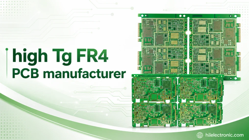
High Tg FR4 PCB Manufacturer for Industrial, Automotive, and Power Electronics
High Tg FR4 PCB manufacturing is usually driven by a...
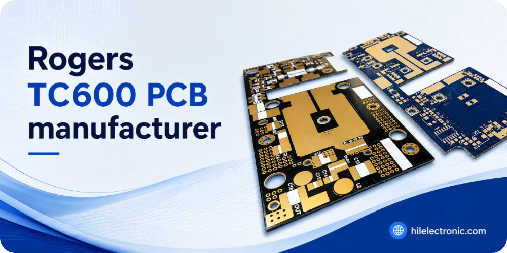
Rogers TC600 PCB Manufacturer for High-Dk and High Thermal Conductivity RF Boards
Rogers TC600 PCB manufacturing is usually requested when a...
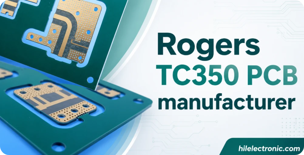
Rogers TC350 PCB Manufacturer for RF Power Amplifier Boards
Rogers TC350 PCB manufacturing is usually requested for...
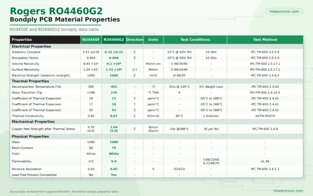
Rogers RO4460G2 Bondply PCB for High-Dk Multilayer RF Stackups
Rogers RO4460G2 bondply PCB projects are usually not...