
Comprehensive Guide to PCB Design Files and Communication

Designing a Printed Circuit Board (PCB) involves multiple steps, from creating the circuit schematic to finalizing the physical layout. The successful communication of PCB design decisions to manufacturers or collaborators depends on various file formats that carry crucial information about the design. These files include schematics, Bill of Materials (BOM), PCB layouts, and stack-up design data. To ensure compatibility across different electronics design software, standardized file formats like Gerber files have become industry standards.
This detailed guide will walk you through the types of files required for PCB design and how they help in communicating your design to manufacturers.
Understanding Gerber Files and Interoperability in PCB Design
One of the biggest challenges in PCB design is ensuring that designs can be understood and manufactured regardless of the specific software used to create them. There are many software platforms for PCB design, including Altium Designer, Allegro, Eagle, KiCAD, and others. To ensure interoperability between these systems, Gerber files were developed.
Gerber files are a universal standard for PCB designs, allowing manufacturers to interpret your design without being locked into a specific software format. Essentially, they describe the layers of a PCB, including copper traces, solder masks, silkscreens, and drill data.
There are different versions of Gerber files, including:
- RS-274X (Gerber X1): This is one of the most widely used formats for PCB fabrication.
- Gerber X2: An advanced version of Gerber that includes metadata like layer type and pad function.
- IPC-2581: An open standard for PCB design data that includes both Gerber and BOM information.
- ODB++: A CAD-to-CAM exchange format that combines all PCB layers and manufacturing data into a single file.
Using these formats allows seamless communication between design engineers and PCB manufacturers, ensuring that all necessary information is conveyed clearly and accurately.
Key File Types for PCB Design
To ensure the smooth transition from design to manufacturing, there are a few essential files you must generate. Each type of file serves a distinct role in communicating different aspects of your design.
1. Gerber Files (RS-274X or X2)
Gerber files are the most crucial files in the PCB manufacturing process. They define the physical layers of the PCB and contain all the information about copper traces, solder masks, and component placements.
The Gerber file includes data for:
- Copper Layers: Which outline the electrical connections on the PCB.
- Solder Mask Layers: Indicating areas where solder resist will be applied to protect the copper traces.
- Silkscreen Layers: Containing component labels, logos, or part identifiers that are printed on the surface of the PCB.
- Drill Files: Describing the positions and sizes of holes or vias on the PCB.
By providing Gerber files, you ensure that the manufacturer can precisely recreate your PCB according to your design.
2. Bill of Materials (BOM)
The Bill of Materials (BOM) is essential for PCB assembly, as it lists all the components required to populate the board. Without a proper BOM, the assembly process cannot proceed, as the manufacturer wouldn’t know which parts to use.
A BOM typically contains:
- Component Name: The specific part identifier (e.g., resistors, capacitors).
- Manufacturer Part Number (MPN): The manufacturer’s unique part number for each component.
- Quantity: The number of each component required for the design.
- Description: Details about the component, such as resistance value, voltage rating, or tolerance.
- Manufacturer: The name of the company that produces the component.
- Alternative Parts: Optional, listing alternative components that can be used if the primary part is unavailable.
The BOM should be provided in commonly accepted formats, such as:
- TXT
- CSV
- XLS
In addition to Gerber files and the BOM, there are other file types that provide more specific information about the mechanical structure and schematic details of the PCB.
3. Mechanical Files (DXF, STEP, DWG)
Mechanical files are essential for defining the physical structure of your PCB, including its shape, size, and other mechanical features such as cutouts, mounting holes, or special contours. These files ensure that the PCB fits properly within its enclosure and that any physical constraints are respected.
Mechanical files typically include:
- PCB Outline: Defines the exact shape and dimensions of the PCB.
- Mounting Holes and Cutouts: Specifies the locations and sizes of any holes or cutouts.
- Panelization: If the board is to be manufactured in panels, mechanical files may also include panelization details.
The most common file formats for mechanical files are:
- DXF: A widely used CAD file format for defining 2D shapes and structures.
- STEP: A 3D model format that allows the manufacturer to visualize and manipulate the physical board in a 3D environment.
- DWG: Another CAD format similar to DXF, commonly used in AutoCAD.
Providing accurate mechanical files helps prevent issues such as improper board fitting, misaligned cutouts, or incorrect mounting hole placement.
4. 3D Assembly Drawings (STEP or 3D PDF)
While Gerber files and mechanical files are crucial, providing a 3D assembly drawing is highly recommended, especially for complex designs with tight tolerances or critical component placement. A 3D assembly drawing offers a visual representation of how the PCB and its components will look once assembled. This file type can help the manufacturer:
- Visualize Component Placement: Ensuring all parts fit correctly and that there are no physical conflicts.
- Check for Clearance Issues: Verifying that components will not interfere with each other or with the enclosure.
- Improve Communication: A 3D model allows for more precise communication between you and the manufacturer, reducing the risk of misunderstandings.
The most common formats for 3D assembly drawings are:
- STEP (.step or .stp): A widely used 3D model format that is compatible with most CAD tools and can represent the full assembly, including components.
- 3D PDF: A PDF format that allows you to embed interactive 3D models, making it easy to share and review without specialized CAD software.
Providing a 3D assembly drawing ensures that the manufacturer has a clear understanding of how the final product will look, reducing the risk of assembly errors.
Comprehensive Summary of PCB Design File Formats for Submission
When preparing to submit your PCB design to a manufacturer, it is important to provide all the necessary files that detail every aspect of your design. These files include layer information, component lists, mechanical dimensions, and more. Each file type plays a key role in ensuring the successful fabrication and assembly of the PCB.
Here is a comprehensive table of the required file types, formats, and descriptions that must be submitted to the PCB manufacturer, along with the associated .pcb file types that are commonly generated by PCB design software.

At Highleap Electronic, we pride ourselves on our ability to work with all major PCB file formats from the industry’s leading design tools, including Altium Designer, Cadence Allegro, Eagle, KiCAD, and others. Our extensive support for these formats ensures that your design can be seamlessly transitioned from the design stage to manufacturing without file compatibility issues.
We ensure precision and quality in all aspects of PCB manufacturing by accepting these formats, from the initial Gerber file submission to the 3D assembly drawings that confirm your board’s final form. By providing flexibility in file types, we help you focus on your design while we handle the technicalities of fabrication and assembly.
Verification and DFM (Design for Manufacturability) Checks
At Highleap Electronic, we offer free DFM (Design for Manufacturability) checks to ensure that your PCB design is ready for production. Our DFM checks are designed to identify potential issues that could affect manufacturability, helping you avoid costly errors and delays before fabrication begins.
By running these checks, we can detect and address issues such as:
-
Insufficient Trace Widths: Ensuring that all copper traces are wide enough to carry the necessary current without causing overheating or failures.
-
Improper Solder Mask Clearances: Verifying that the clearances between copper pads and the solder mask are correct to prevent unintended solder bridging and short circuits during assembly.
-
Overlapping Components: Ensuring there is enough space between components to prevent assembly problems, particularly for automated placement and soldering processes.
-
Via and Hole Size Issues: Confirming that all vias and through-holes meet the manufacturer’s drill size and aspect ratio requirements to ensure reliable fabrication and functionality.
-
Copper-to-Edge Clearances: Checking that copper traces and pads are positioned far enough from the edge of the PCB to avoid damage or electrical shorts during use.
Our DFM checks are integrated into our manufacturing process and are designed to ensure that your PCB is optimized for fabrication. This service helps catch potential issues early, saving you time and reducing the likelihood of production errors. With our free DFM checks, you can be confident that your design will meet all necessary specifications, making the transition from design to production seamless.
By utilizing Highleap Electronic’s free DFM checks, you can rest assured that your PCB will be manufacturable, reliable, and cost-effective, ensuring that your project moves forward smoothly.
Effective PCB Production: Version Control and File Management
Version Control and File Management
Maintaining proper version control is crucial in PCB design to ensure that the correct files are used for fabrication and assembly. As designs go through multiple iterations, manufacturers may receive different versions of the same project. To prevent confusion and ensure that the latest version is always fabricated, it’s essential to adopt a clear and consistent labeling system. This can include version numbers (e.g., V1.0, V2.1), revision dates, and notes on significant changes made to the design. Proper version control allows both the design team and the manufacturer to track updates easily, ensuring that outdated files are not mistakenly used during production.
Additionally, consistency in file naming conventions plays a key role in avoiding miscommunication. Each file should clearly indicate its purpose (e.g., “PCB_v2.1_top_layer.gbr” or “BOM_v2.0_Jan2024.csv”) to ensure that all parties involved—engineers, manufacturers, and procurement teams—can quickly identify and access the correct files. This approach not only prevents costly errors during manufacturing but also simplifies collaboration and quality control throughout the production process.
File Transfer and Communication with Manufacturers
Once all design files are finalized, it’s important to transfer them securely to your manufacturer. A best practice is to organize all relevant files (Gerbers, BOM, mechanical files, 3D models, drill files, etc.) into a single compressed ZIP package. This ZIP file should include a clear, detailed readme file that explains the contents of the package and provides any special instructions for fabrication or assembly. This organized approach ensures that the manufacturer has access to all the necessary information without confusion or missing files.
Effective communication with the manufacturer is equally important. Regular and proactive communication allows the manufacturer to clarify any uncertainties or ask questions about specific aspects of the design, such as tolerances, materials, or production techniques. Keeping an open line of communication also helps prevent delays and production errors, ensuring that the entire process runs smoothly. Providing manufacturers with clear instructions, being responsive to their inquiries, and confirming design details early in the process fosters a strong collaboration, leading to successful PCB production.

Conclusion
Designing a PCB is more than just creating the physical board—it’s about effectively managing and communicating the flow of information between the designer and the manufacturer. Each file type, from Gerbers to BOMs and 3D models, plays an essential role in ensuring that your PCB is fabricated and assembled correctly.
At Highleap Electronic, we support a wide range of PCB file formats, including Gerber files, native PCB design files, mechanical files, and 3D assembly models. By providing flexibility and ensuring precision throughout the process, we help bridge the gap between design and producti

Recommended Posts

PCB Current Calculator: Sizing Trace Width and Vias with the IPC-2221 Formula
Figure 1. Pcb Current Calculator reference image for PCB...
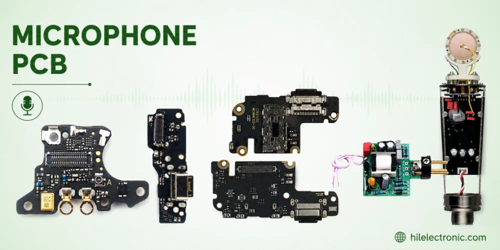
Microphone PCB Design: How the Board Itself Shapes Your Audio Quality
Figure 1. Microphone Pcb reference image for PCB...
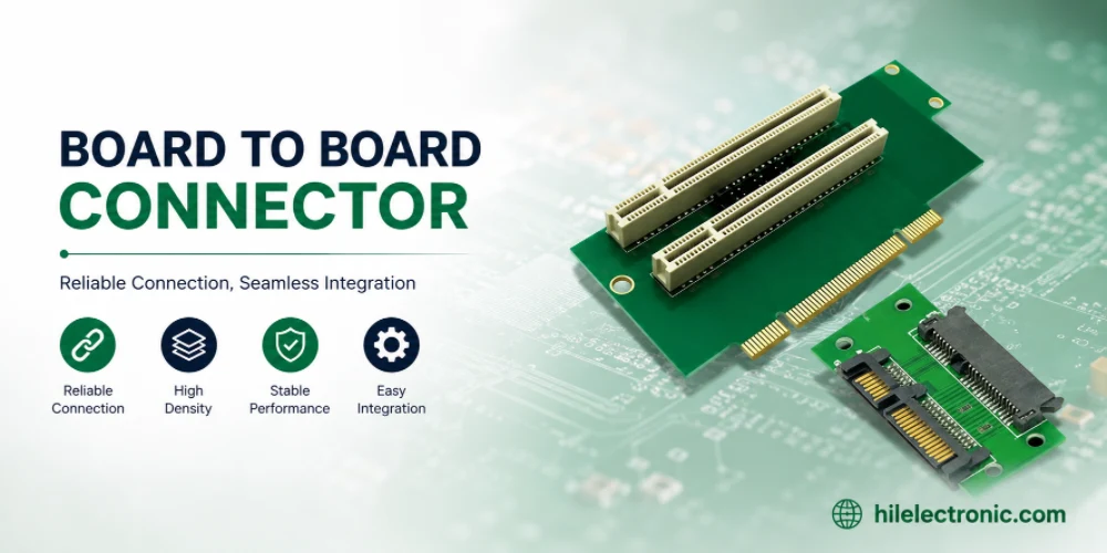
Board-to-Board Connector: Types, Specifications, and How to Select One
Figure 1. Board To Board Connector reference image for PCB...
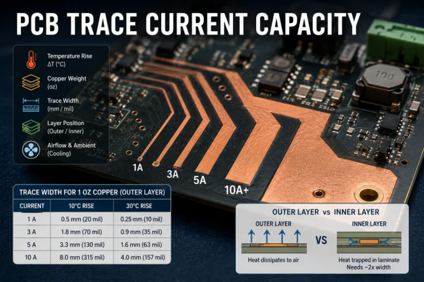
PCB Trace Width Calculator: How to Size Traces for Current, Voltage Drop, and Impedance
Figure 1. A PCB trace width calculator is a starting point...