
Back to blog
PCB Design Specifications for Switching Power Supplies

Switching Power Supplies PCBA
Designing a switching power supply (SPS) PCB demands meticulous attention to detail to ensure stable operation and minimize electromagnetic interference (EMI). From schematic to layout, every step is critical. This comprehensive guide explores key considerations and best practices for designing an efficient and reliable SPS PCB.
Schematic to PCB Design Flow
The transition from schematic to PCB design involves several critical steps:
- Establish Component Parameters: Define the specifications for each component, considering voltage, current, and frequency requirements.
- Input Schematic Netlist: Transfer the schematic into a netlist format that can be used for PCB layout.
- Design Parameter Settings: Configure the PCB design software with the necessary parameters, including trace widths, clearances, and layers.
- Manual Layout: Arrange the components on the PCB according to the schematic and design requirements.
- Manual Routing: Route the traces between components, ensuring proper spacing and avoiding interference.
- Design Validation: Verify the design for electrical and mechanical integrity, including signal integrity and thermal considerations.
- Review: Conduct a thorough review of the design to ensure it meets all requirements.
- CAM Output: Generate the final output files for manufacturing.
Circuit Board Layout Parameters for Switching Power Supplies
To ensure optimal power integrity in switching power supply (SPS) designs, careful consideration must be given to the circuit board layout. The following parameters are crucial for designing a robust power delivery network (PDN) that can provide clean and uninterrupted power to all components while minimizing interference:
- Board Layer Configuration and Stackup: Start with a schematic that identifies all power supplies on the board. Configure the layer stackup to optimize signal and power integrity. Position power and ground planes for optimal signal return paths, controlled impedance routing, and power supply isolation.
- Design Rules and Constraints: Establish rules for trace width, spacing, and copper pour attributes. Consider using net classes to manage these rules efficiently. Advanced PCB design tools, such as Cadence Allegro’s PCB Editor, offer capabilities to support the routing requirements of the PDN.
- Placement and Routing Guidelines: Follow these guidelines for switching power supplies:
- Component Placement: Place components to minimize trace lengths and optimize signal paths. Keep high-current components close to their respective decoupling capacitors to minimize inductance.
- Routing: Route power traces as wide as possible to reduce resistance and voltage drop. Use multiple vias for high-current paths to reduce resistance and improve thermal performance. Keep high-current loops short and compact to minimize EMI.
- Decoupling Capacitors: Place decoupling capacitors as close as possible to the power pins of the components they are decoupling to provide a low-impedance path for high-frequency noise.
- Grounding: Implement a solid ground plane to provide a low-impedance return path for currents. Use stitching vias to connect different ground layers and minimize ground loops.
- Signal Integrity: Use controlled impedance routing for high-speed signals to minimize signal reflections and ensure signal integrity.
By carefully considering these parameters and guidelines, you can design a PCB layout that maximizes power integrity and minimizes interference in switching power supply applications.

Switching Power Supplies PCB layout
Switching Power Supplies Component Layout
When laying out components, consider the PCB size as a priority. An oversized PCB can lead to longer trace lengths, increased impedance, reduced anti-noise capability, and higher costs. Conversely, an undersized PCB may suffer from poor heat dissipation and increased interference. The optimal shape for a PCB is rectangular, with a length-to-width ratio of 3:2 or 4:3. Components placed near the board’s edge should be at least 2mm away to avoid potential issues.
In component placement, prioritize future soldering considerations and avoid overly dense arrangements that could impede soldering processes. Arrange components uniformly, neatly, and compactly around the core components of each functional circuit. Minimize and shorten lead wires and connections between components, and place decoupling capacitors as close to the VCC of the component as possible.
Consider the distribution parameters between components, especially for circuits operating at high frequencies. Components should be arranged as parallel as possible to facilitate soldering and mass production. Arrange the positions of each functional circuit unit according to the circuit flow to ensure the layout is conducive to signal circulation and maintains signal consistency. Finally, ensure routing fluency as the primary layout principle, paying attention to flying wire connections and placing components with interconnections together to minimize signal path lengths.
Optimizing Grounding for Stable Switching Power Supply Operation
Switching power supplies contain high-frequency signals, and any printed line on the PCB can act as an antenna. The length and width of the printed line affect its impedance and reactance, thereby influencing the frequency response. Even printed lines carrying DC signals can couple to RF signals from nearby printed lines and cause circuit problems (or even re-radiate interference signals).
To mitigate this, all AC-carrying printed lines should be designed as short and wide as possible. This implies that all components connected to printed lines and other power lines should be placed as close as possible. The length of the printed line is proportional to its inductance and impedance, while the width is inversely proportional to its inductance and impedance. The longer the length, the lower the frequency at which the printed line can transmit and receive electromagnetic waves, and the more RF energy it can radiate.
Therefore, it’s crucial to carefully consider the placement of the ground wire in the layout to avoid mixing various grounds, which can lead to unstable power supply operation. Grounding plays a vital role as the common reference point for the four current loops of the switching power supply and is an important method for controlling interference. Here are some key points to note in ground design:
- Select single-point grounding: The common terminal of the filter capacitor should be the only connection to the common ground coupled to the large current AC ground. Ground points of the same-level circuit should be as close as possible, and the filter capacitor of the main circuit should also be connected to the ground point of the level.
- Thicken the ground wire: Ensure that each terminal of a large current uses a printed wire that is as short and wide as possible. The width of the power and ground lines should be widened as much as possible, with the ground line preferably wider than the power line. The relationship between their widths should be: ground line > power line > signal line. If possible, the width of the ground wire should be greater than 3mm.
- Global routing principles: Follow these principles when conducting global routing:
- Routing direction: Keep the orientation of components consistent with the schematic diagram, and the routing direction should be consistent with the circuit diagram.
- Minimize the number of turns in the routing, avoid sudden changes in line width, and ensure wire corners are ≥90 degrees.
- Avoid crossing circuits in the printed circuit. Use methods like “drill” or “loop” to solve potential crossing problems.
- Input and output ground: For a low-voltage DC-DC switching power supply, both sides of the circuit should have a common reference ground. After copper plating both sides of the ground wire, they should be connected together to form a common ground.
Essential Checks for Wiring and Grounding in PCB Design
After the wiring design is completed, it is necessary to carefully check whether the wiring design complies with the rules established by the designer, and also to confirm whether the established rules meet the requirements of the PCB production process. Generally, check whether the distances between lines and lines, lines and component pads, lines and through-holes, component pads and through-holes, and between through-holes are reasonable and meet production requirements.
Check if the width of the power and ground lines is appropriate, and if there are any places in the PCB where the ground lines can be widened. Note: Some errors can be ignored, such as part of the outline of some connectors being placed outside the board frame, which can cause errors in spacing checks; also, after each modification to the wiring and through-holes, the copper should be recoated.
Final Design Checks
Recheck against the “PCB Checklist” which includes design rules, layer definitions, trace widths, spacing, pads and via settings. In addition, focus on reviewing the rationality of component placement, routing of power and ground networks, routing of high-speed clock networks, shielding, placement and connection of decoupling capacitors, etc.
Design output considerations for photomask file output:
A. The output layers include wiring layer (bottom layer), silk screen layer (including top layer and bottom layer silk screen), solder mask layer (bottom solder mask layer), drilling layer (bottom layer), and drilling files (nc drilling) are also generated.
B. When setting the number of silk screen layers, do not select the part type; select the outline, text, and lines of the top (bottom) and silk screen layers.
C. When setting layers for each layer, select the board outline; when setting the number of layers for the silk screen layer, do not select the part type; select the outline, text, and lines of the top (bottom) and silk screen layers.
D. When generating drilling files, use the default settings of PowerPCB without making any changes.
PCB & PCBA Quick Quote
Related Articles
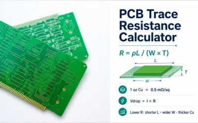
PCB Trace Resistance Calculator: How to Calculate Trace Resistance and Voltage Drop
Calculate PCB trace resistance, voltage drop, power loss, and copper width choices for reliable fabrication and power delivery.
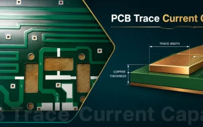
PCB Trace Current Capacity: Width, Copper Weight, and IPC-2221
Learn PCB trace current capacity by copper weight, trace width, layer position, voltage drop, and DFM limits before ordering a board.

EAGLE PCB Software: Is It Free, EAGLE vs KiCad, and How to Export Gerber Files
Compare EAGLE PCB software with KiCad and Altium, then export Gerber, drill, and assembly files for PCB manufacturing review.