
Advantages and Considerations of 4-Layer PCB Fabrication
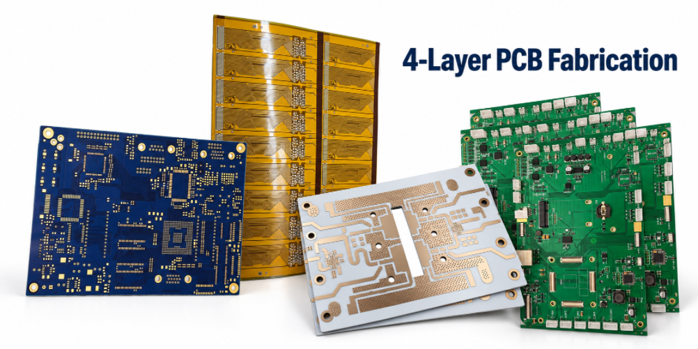
Highleap Electronics provides 4-layer PCB manufacturing and assembly for standard circuit boards, specialized materials and application-specific constructions. Our product scope covers rigid, flexible and rigid-flex designs, high-frequency and high-speed circuits, HDI structures, and specified manufacturing requirements.
From prototypes and low-volume orders to repeat production and larger manufacturing runs, each project is evaluated according to its material, stackup, dimensions, copper weight, tolerances and required processes. Submit your design files and specifications for manufacturing review and a project-specific quotation.
On This Page
Need a 4-Layer PCB Quote?
Send your fabrication files and board specifications for review.
4-Layer PCB Products and Manufacturing Options
Highleap’s four-layer PCB product scope covers different board structures, material systems, physical specifications, surface finishes and fabrication processes. The following categories help define your requirements for quotation and engineering review. Individual options may be combined where the resulting construction is compatible with the applicable manufacturing process.
PCB Structures
- 4-layer rigid PCB
- 4-layer flexible PCB / FPC
- 4-layer rigid-flex PCB
- 4-layer HDI PCB
- Hybrid-material PCB constructions
- Ceramic substrate constructions
- Metal-core constructions, subject to feasibility review
Materials and Electrical Performance
- FR-4 4-layer PCB
- High-Tg 4-layer PCB
- High-speed PCB
- High-frequency and RF PCB
- Low-loss material constructions
- Rogers and PTFE material systems
- Taconic and other specified laminates
- Halogen-free PCB materials
- Controlled-impedance constructions
- Specified-grade and mixed-material stackups
Dimensions and Physical Specifications
- Large-format 4-layer PCB
- Long flexible PCB constructions
- Thick and ultra-thin boards
- Heavy-copper 4-layer PCB
- Fine-line and fine-spacing designs
- Special outlines and cutouts
- Irregular board shapes
- Specified finished-thickness tolerances
- Special copper-weight combinations
- Application-specific dimensional requirements
Special Processes and Order Types
- Blind-via and buried-via constructions
- Microvias and via-filled structures, where supported
- Quick-turn prototypes, subject to schedule
- Low-volume and pilot production
- Mass production and recurring orders
- PCB fabrication with assembly
- Specified inspection and documentation
Surface Finish and Solder Mask Options
- Green, black, white and other specified solder mask colors
- Silkscreen color and legend requirements
- ENIG, lead-free HASL and OSP
- Immersion silver and immersion tin, where available
- Gold fingers and selective finishing, where applicable
- Surface finish thickness requirements
- Specified solderability and cosmetic acceptance criteria
Advanced Fabrication Features
- Backdrilling for specified high-speed designs
- Copper-filled and resin-filled vias, where supported
- Plated through-holes and non-plated holes
- Counterbore and countersink features, where applicable
- Controlled-impedance fabrication requirements
- Special drilling and dimensional tolerances
- Engineering-reviewed process combinations
These categories can overlap within the same design. A four-layer PCB may combine a specified laminate with controlled impedance, a particular copper weight, special drilling and a defined surface finish. The complete construction, rather than an individual product label, determines manufacturing feasibility.
Manufacturing scope: Specialized ceramic, metal-core, rigid-flex, HDI and other non-standard constructions require confirmation against actual process capabilities. Specify the required structure and material grade when requesting a quotation.
4-Layer PCB Fabrication and Assembly
Four-layer PCB fabrication involves inner-layer circuit formation, layer registration, lamination, drilling, plated-hole formation, outer-layer processing, solder mask, surface finishing and final inspection. The production route depends on the selected construction, material system, feature dimensions and required tolerances.
Material Preparation and Layer Construction
The laminate, copper weights and dielectric arrangement must support the required finished thickness and electrical performance. The stackup defines the relationship between conductive layers and insulating materials. For controlled-impedance boards, dielectric properties, copper thickness, trace geometry and reference-plane arrangement must be evaluated together.
Where a particular laminate grade is mandatory, identify the manufacturer and grade in the fabrication documentation. If equivalent materials may be considered, specify the electrical, thermal and compliance requirements that any alternative must meet. Substitutions should be reviewed and approved before use.
Drilling, Plating and Circuit Formation
Drilling and plating establish the electrical interconnections required by the design. Hole diameter, plating requirements, annular rings, clearances and via structures must be compatible with the specified construction. Blind vias, buried vias, microvias, backdrilling and filled vias may require additional process checks.
After circuit formation, solder mask, silkscreen and the selected surface finish are applied according to the fabrication specification. The finish should be chosen with consideration for component assembly, solderability, storage requirements and the intended application.
PCB Assembly Coordination
When populated boards are required, fabrication should be coordinated with component sourcing, placement, soldering and testing. The assembly package should identify the BOM, pick-and-place data, assembly drawings, component requirements and any required functional verification. These details allow the bare-board specification and finished PCBA requirements to be evaluated together.
Prototype, low-volume, repeat-order and larger production requirements can be assessed according to the project. Actual lead time depends on construction complexity, material availability, order quantity and the confirmed production schedule.
4-Layer PCB Design Requirements and DFM Review
A complete fabrication package helps the manufacturing team assess the design, identify missing information and determine whether the specified construction is feasible. Inconsistent files, unclear tolerances or incomplete stackup information can delay quotation and production, particularly for boards with fine features or specialized materials.
Fabrication Files and Technical Specifications
For an initial manufacturing review, prepare the latest available versions of the following files and specifications:
- Gerber files or another agreed fabrication-data format, together with NC drill files
- Board outline, finished dimensions, cutouts and thickness
- Layer stackup, laminate grade and copper weight for each layer
- Surface finish, solder mask color and silkscreen requirements
- Minimum trace width, spacing, drill sizes and critical tolerances
- Controlled-impedance targets and relevant layer details, if required
- Special via structures, backdrilling or filling requirements, where applicable
- Quantity, target delivery date and acceptance criteria
Design-for-Manufacturing Checks
DFM checks should evaluate whether the supplied files, drawings and stackup are consistent with the requested manufacturing process. Relevant considerations include copper clearances, annular rings, drill-to-copper spacing, minimum features, board-edge requirements and compatibility between the selected material and construction.
For controlled-impedance boards, provide the target values, tolerances and relevant signal-layer information. Flexible and rigid-flex designs require appropriate construction details, while specialized materials should be identified by exact grade wherever possible.
Any proposed design adjustments or material substitutions should be discussed and approved before they are incorporated into the production data. A manufacturability review helps identify potential issues, but it does not replace approval of the final design and specifications.
Before submitting files: Confirm that the fabrication package matches the latest drawing revision. Clearly distinguish mandatory requirements from preferences that may be evaluated during engineering review.
4-Layer PCB Quality Control and Testing
Quality planning should reflect the board construction, critical dimensions, intended application and customer acceptance criteria. Four-layer PCB inspection may cover inner-layer patterns, registration, plated holes, outer-layer circuitry, solder mask, surface finish and finished dimensions. The applicable controls depend on the approved specification.
Visual and Dimensional Inspection
Inspection may include circuit-pattern checks, layer alignment, hole locations, board outline, solder mask registration and other specified features. For multilayer boards, layer registration and interconnection quality are important considerations. Acceptance limits should be defined by the drawing and purchase specification rather than assumed to be identical for every order.
Electrical Testing and Impedance Verification
Bare-board electrical testing can be specified to verify continuity and isolation. When controlled impedance is required, the target values, tolerances and verification requirements should be agreed before production. Additional testing or reporting may be needed for designs with particular electrical or reliability requirements.
For assembled boards, inspection and testing may also cover component placement, solder joints and functional performance. The appropriate methods depend on the PCBA design and agreed acceptance criteria.
Inspection Records and Acceptance Requirements
If the order requires material certifications, inspection reports, electrical test records or traceability documentation, include these items in the quotation request. Defining required records and acceptance criteria before production helps align manufacturing, inspection and delivery expectations.
Quality controls should be selected according to the project rather than treated as automatic guarantees. Where a particular test or report is mandatory, confirm its scope and acceptance limits with the manufacturing team before the order is released.
4-Layer PCB Assembly and Manufacturing Quote
A reliable quotation must reflect the complete board specification rather than layer count alone. Board dimensions, material grade, copper weight, finished thickness, minimum features, surface finish, special processes, inspection requirements, quantity and delivery target can all influence manufacturing cost and lead time.
Information Required for a Fabrication Quote
Submit the latest fabrication files along with the stackup, material requirements, finished dimensions, copper weights, surface finish, quantity and target delivery date. Include drawings and special process notes for high-frequency, flexible, rigid-flex, HDI or other non-standard constructions. If a material grade is mandatory, identify it explicitly and state whether equivalent alternatives may be considered.
For a more accurate estimate, distinguish required specifications from preferences that may be reviewed during engineering assessment. This helps the quotation team identify missing information, evaluate feasibility and determine whether clarification is needed before pricing can be finalized.
PCB Assembly and Turnkey Requirements
For assembly orders, also provide the BOM, pick-and-place file, assembly drawings and test instructions. Component sourcing, package types, placement complexity and inspection requirements can affect the assembly quotation independently of the bare-board cost.
Highleap provides PCB assembly services for projects requiring component placement after board fabrication. If both bare boards and assembled units are needed, include the requirements for each stage so the complete project scope can be evaluated.
Cost and Production Schedule
PCB pricing depends on technical specifications and order conditions. Material availability, board complexity, panel utilization, special processes, inspection requirements and quantity can affect the final quotation. Assembly pricing additionally depends on component procurement, BOM complexity, placement requirements and testing scope.
Lead time should be confirmed against the actual board design, material availability and production schedule. For repeat orders, keeping the approved revision, material specification and acceptance criteria consistent can reduce avoidable clarification between production runs.
Request a 4-Layer PCB Manufacturing Quote
Send your Gerber files, stackup, material specifications, quantity and delivery target to Highleap Electronics for manufacturing review and quotation. For assembly projects, include your BOM and assembly data as well.

Recommended Posts
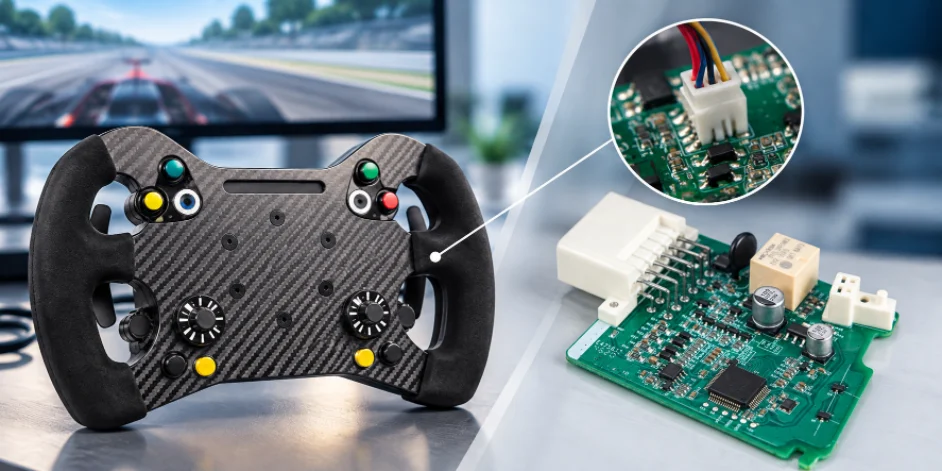
Racing Wheel Controller PCB Manufacturing & Assembly for Force-Feedback and Direct-Drive Gaming Systems
Highleap Electronics provides PCB fabrication and PCBA for...

FR4 Dielectric Constant Calculator and PCB Design Guide
How to get a quote for PCBs Let's run DFM/DFA analysis for...

GPS Sports Watch PCB Design: GNSS, RF, Sensors and PCBA Manufacturing
Turning a compact GPS sports watch controller from an...

Cellular Modem PCB: From Module Carriers to PCBA
Need a manufacturer for a cellular modem PCB or a fully...