
About the application of inverters PCB

Defining Low and High-Frequency Inverters
Inverters are devices that convert direct current (DC) into alternating current (AC). They play a crucial role in renewable energy systems, especially solar power systems, where the generated power is often in DC form and needs to be converted to AC for household or grid use. Based on the frequency of operation, inverters can be classified into low-frequency inverters and high-frequency inverters:
Low-Frequency Inverters
Low-frequency inverters operate with switching frequencies close to the AC line frequency (50/60Hz). The switching frequencies for these inverters typically range from 100 Hz to 5 kHz.
Characteristics
- Topology: Full-bridge topology is commonly used.
- Semiconductors: BJTs, MOSFETs, and IGBTs are typically employed for switching.
- Filter Components: Large inductors and capacitors are required to filter the output.
- Frequency Ratio: The ratio between switching and output frequency can be up to 1:100.
- Control Complexity: Control schemes are relatively simple, usually involving open-loop voltage control.
High-Frequency Inverters
High-frequency inverters operate at much higher switching frequencies, usually ranging from tens of kHz to MHz.
Characteristics
- Topology: Full-bridge topology is also commonly used, similar to low-frequency inverters.
- Semiconductors: MOSFETs and IGBTs are generally used, capable of fast switching.
- Filter Components: Smaller inductors and capacitors are sufficient for output filtering due to the high switching frequency.
- Frequency Ratio: These inverters can have a frequency ratio ranging from 1:1000 to 1:50,000.
- Control Complexity: A more complex, high-speed control scheme is needed due to the high switching frequencies.
Key Differences and Considerations
- Topology: Both types commonly use a full-bridge topology, but the components and control strategies differ.
- Switching Frequency: Low-frequency inverters operate closer to the line frequency, while high-frequency inverters operate at much higher frequencies, affecting various other parameters like filter size and efficiency.
- Frequency Ratio: High-frequency inverters have a much higher ratio between the switching frequency and the output frequency, allowing for better performance metrics in certain applications.
- Filter Size: The filter components in low-frequency inverters are generally much larger due to the lower switching frequencies.
- Semiconductors: While both types can use MOSFETs and IGBTs, low-frequency inverters can also use BJTs, which are generally not suitable for high-frequency applications.
- Control Complexity: High-frequency inverters require more complex control algorithms to manage the high-speed switching.
- Efficiency: High-frequency inverters are generally more efficient, benefiting from lower conduction and switching losses.
- Power Density: High-frequency inverters are more compact and offer higher power density, making them suitable for portable or space-constrained applications.
- Distortion: High-frequency inverters usually produce outputs with lower harmonic distortion.
- Response Speed: High-frequency inverters can react more quickly to changes in load or input conditions.
- Physical Size and Weight: High-frequency inverters are generally smaller and lighter, thanks to the reduced size of filter components and higher power density.
- Applications: While both types have broad application spectra, their inherent characteristics make them more suitable for specific use-cases.
Understanding these fundamental definitions and characteristics helps in determining which type of inverter is best suited for specific needs.

Low-Frequency Inverters PCB Design Considerations
Designing the PCB for low-frequency inverters involves several critical considerations to ensure reliable and efficient operation. Here are some key PCB design considerations for low-frequency inverters:
- Layer Stackup: Determine the appropriate layer stackup for your PCB. Low-frequency inverters may not require as many layers as high-frequency designs but consider using multiple layers for signal integrity, power distribution, and grounding.
- Grounding: Implement a solid grounding strategy. Proper grounding is crucial for minimizing noise and ensuring stable performance. Use separate ground planes for analog and digital components and connect them at a single point to avoid ground loops.
- Component Placement: Carefully place components on the PCB. Group related components together and keep high-power components away from sensitive analog or digital circuitry to prevent interference. Consider the heat generated by power components and add thermal relief measures.
- Power Distribution: Design a robust power distribution network. Ensure that power traces are adequately sized to handle the required currents without excessive voltage drop. Place bypass capacitors strategically to filter out noise.
- Signal Routing: Pay attention to signal routing. Minimize trace lengths and use wide traces for high-current paths. Route critical signals away from noise sources and follow best practices for signal integrity.
- Protection Circuitry: Include protection circuitry on the PCB to safeguard against overcurrent, overvoltage, and over-temperature conditions. Ensure that protection circuits are well-integrated into the design and can respond quickly to faults.
- EMI and EMC Considerations: Address electromagnetic interference (EMI) and electromagnetic compatibility (EMC) issues. Use proper filtering and shielding techniques to minimize emissions and susceptibility to interference. Follow relevant regulatory standards.
- Thermal Management: Plan for effective thermal management. Even though low-frequency inverters generate less heat than high-frequency ones, power components can still get hot. Use suitable heatsinks and ensure adequate airflow or passive cooling.
- Isolation: If isolation is required, incorporate isolation transformers or optocouplers into the design, ensuring proper separation between input and output sections.
- Component Selection: Select components that are suitable for low-frequency operation. Pay attention to voltage and current ratings, as well as temperature ratings for components like capacitors and inductors.
- Safety Features: Integrate safety features such as fuses, circuit breakers, or fault detection circuits to protect both the inverter and connected equipment. Ensure that the PCB design adheres to safety standards.
- Testing and Debugging: Include test points or access points on the PCB for debugging and testing during the design and manufacturing process. This facilitates troubleshooting and validation.
- Documentation: Create comprehensive PCB design documentation that includes schematics, a bill of materials (BOM), layout guidelines, and assembly instructions to facilitate manufacturing and maintenance.
- Manufacturability: Consider manufacturability factors such as component availability, assembly techniques, and solderability to ensure the PCB can be efficiently manufactured.
- Compliance: Ensure that the PCB design complies with relevant safety and regulatory standards for low-frequency power electronics applications.
- Environmental Considerations: Take into account environmental conditions, such as temperature variations and humidity, in which the inverter will operate, and design the PCB to withstand these conditions.
Designing a PCB for low-frequency inverters requires a solid understanding of power electronics and PCB layout techniques. Collaboration with experienced PCB designers and simulation experts can be valuable in achieving a successful low-frequency inverter PCB design. Additionally, thorough testing and validation are essential to ensure that the PCB performs as expected in low-frequency applications.

High-Frequency Inverters PCB Design Considerations
Designing the PCB for high-frequency inverters requires careful attention to various factors to ensure the reliability, performance, and efficiency of the inverter. High-frequency inverters operate at frequencies well above the standard 50 Hz or 60 Hz and often require special considerations for PCB layout and design. Here are some key PCB design considerations for high-frequency inverters:
- Layer Stackup: Consider the layer stackup of the PCB. High-frequency designs often require multilayer PCBs to provide proper grounding, power distribution, and signal integrity. Controlled impedance layers may also be necessary for specific high-frequency traces.
- Grounding: Implement a solid grounding scheme. High-frequency circuits are sensitive to ground loops and noise. Separate analog and digital ground planes and use a star grounding topology to minimize interference.
- Signal Integrity: Pay close attention to signal integrity. High-frequency inverters require careful control of trace lengths, impedance matching, and minimizing parasitic capacitance and inductance. Use controlled impedance traces for critical high-frequency signals.
- Component Placement: Place components strategically. Group related components together to minimize trace lengths and reduce parasitic effects. Keep high-power components away from sensitive analog or digital circuitry to prevent interference.
- Thermal Management: Plan for effective thermal management. High-frequency inverters can generate significant heat, especially in power components and high-current traces. Use appropriate heatsinks, thermal vias, and consider forced air cooling if necessary.
- EMI and EMC Considerations: Incorporate EMI/EMC (Electromagnetic Interference/Electromagnetic Compatibility) measures into the PCB design. Use proper shielding, filtering, and grounding techniques to minimize emissions and susceptibility to interference.
- Power Distribution: Ensure a robust power distribution network. High-frequency inverters require stable and clean power supplies. Use low-inductance power traces and bypass capacitors strategically to minimize voltage droops and noise.
- High-Frequency Routing: Route high-frequency signals carefully. Maintain controlled impedance and use differential pair routing for critical signals. Minimize vias and avoid sharp corners in traces to reduce signal reflections and losses.
- Isolation: In applications where electrical isolation is required, consider the placement and design of isolation transformers or optocouplers on the PCB.
- Protection Circuitry: Include protection circuitry on the PCB to safeguard against overcurrent, overvoltage, and over-temperature conditions. Ensure that these protection circuits are well-integrated into the design.
- Component Selection: Select components rated for high-frequency operation and low parasitic effects. High-speed switching devices, high-frequency capacitors, and inductors designed for high-frequency applications are essential.
- Routing and Clearance: Maintain adequate clearance between high-voltage and low-voltage traces to prevent arcing and shorts. Follow safety standards and guidelines for clearance distances.
- Testing Points: Include test points or access points on the PCB for debugging and testing during the design and manufacturing process.
- Simulation and Analysis: Use simulation tools and perform signal integrity and power integrity analyses to validate the PCB design before fabrication. Simulations can help identify and address potential issues early in the design process.
- Documentation: Create comprehensive PCB design documentation that includes schematics, bill of materials (BOM), layout guidelines, and assembly instructions to facilitate manufacturing and troubleshooting.
- Manufacturability: Consider the manufacturability of the PCB design, including factors like component availability, assembly techniques, and solderability.
- Compliance: Ensure that the PCB design complies with relevant safety and regulatory standards for high-frequency power electronics applications.
Designing a PCB for high-frequency inverters requires a deep understanding of power electronics, RF (Radio Frequency) principles, and PCB layout techniques. Collaboration with experienced PCB designers and simulation experts can be valuable in achieving a successful high-frequency inverter PCB design. Additionally, thorough testing and validation are essential to ensure that the PCB performs as expected in high-frequency applications.
Low-Frequency Inverters PCB Applications
Low-frequency inverters find applications in various industries and scenarios where power conversion, voltage regulation, and frequency control at frequencies below 60 Hz are essential. Here are some common applications for low-frequency inverters:
- Off-Grid Power Systems: Used in remote cabins, RVs, and boats, where there is no access to the utility grid. They convert DC power from batteries or renewable energy sources (e.g., solar panels or wind turbines) into AC power for operating appliances and electronics.
- Backup Power Supplies: Employed as backup power supplies during grid outages in residential and commercial settings, often integrated with uninterruptible power supply (UPS) systems.
- Industrial Processes: Used in motor control, welding machines, and power tools, where precise control of motor speed and direction is required.
- Agricultural Equipment: Used in irrigation pumps and grain dryers, converting DC power from solar panels or batteries into AC power for operation in remote locations.
- Telecommunications: Convert DC power from batteries or renewable sources into AC power for communication equipment, repeaters, and base stations in remote areas.
- Emergency Lighting Systems: Provide backup power for critical lighting during power outages in buildings like hospitals, schools, and commercial facilities.
- Hybrid and Electric Vehicles: Convert DC power from the battery to AC power for the electric motor in some hybrid and electric vehicles.
- Renewable Energy Systems: Convert DC power generated by solar panels, wind turbines, or hydroelectric systems into AC power for use in homes, businesses, and utilities.
- Marine and RV Applications: Convert DC power from batteries or generators into AC power for appliances, lighting, and onboard systems in marine vessels and recreational vehicles.
- Mobile Power Generation: Provide reliable AC power for construction sites, outdoor events, and emergency response situations.
- Remote Monitoring Systems: Power sensors, communication equipment, and data loggers in remote monitoring and data acquisition systems.
- Research and Laboratory Equipment: Provide stable and precise AC power sources for scientific instruments and laboratory equipment.
These applications highlight the importance of low-frequency inverters in converting DC power into clean and reliable AC power. The choice of a low-frequency inverter depends on the specific requirements of the application, including power capacity, waveform quality, efficiency, and environmental conditions.

High-Frequency Inverters PCB Applications
High-frequency inverters, operating at frequencies above the standard 50 Hz or 60 Hz range, are used in various applications requiring efficient and precise power conversion. These applications often benefit from the advantages of high-frequency switching, such as smaller components, reduced size and weight, and improved efficiency. Here are some common applications for high-frequency inverters:
- Switch-Mode Power Supplies (SMPS): Convert AC power to DC power or vice versa, commonly found in electronic devices such as computers, televisions, and mobile phone chargers.
- Motor Drives: Employed in variable frequency drives (VFDs) for controlling the speed and torque of electric motors in industrial machinery, HVAC systems, and robotics.
- Solar Inverters: Convert DC power generated by solar panels into AC power for the electrical grid or on-site use in residential and commercial solar installations.
- Wind Turbine Inverters: Convert the variable DC output from wind turbines into grid-compatible AC power.
- Electric Vehicles (EVs) and Hybrid Electric Vehicles (HEVs): Convert DC power from the battery to AC power to drive the electric motor.
- Induction Heating: Used in processes such as metal hardening, forging, and cooking appliances like induction cooktops.
- RF Amplifiers: Provide efficient power amplification for applications like wireless communication, radar, and broadcasting.
- Plasma Cutting and Welding: Generate the high-frequency AC power required for plasma cutting and welding processes.
- Medical Devices: Used in laser systems and diagnostic equipment for precise power control and rapid switching.
- Uninterruptible Power Supplies (UPS): Provide backup power in the event of a grid outage, allowing for rapid switchover to battery power.
- LED Lighting: Drive high-efficiency LED lighting systems, providing precise control of light intensity and color temperature.
- Telecommunications: Used for power conversion and distribution, providing stable and efficient power to networking equipment, base stations, and data centers.
- Aerospace and Defense: Employed in avionics, radar systems, and electronic warfare equipment.
- Laboratory and Research Equipment: Provide precise and stable AC power sources for scientific instruments and research equipment.
- High-Frequency Heating: Used in applications such as microwave ovens and dielectric heating systems for efficient and controlled heating.
These applications highlight the versatility and efficiency of high-frequency inverters in various industries, ranging from consumer electronics to industrial and aerospace applications. The choice of a high-frequency inverter depends on factors like power requirements, efficiency, size constraints, and the specific needs of the application. PCB design for high-frequency inverters in these applications often involves careful consideration of layout, thermal management, and signal integrity to ensure optimal performance.
Why Choose Highleap Electronic for Inverters PCB Production
Highleap Electronic stands out as the premier choice for inverters PCB production due to our commitment to cutting-edge technology, precision engineering, and unmatched expertise in power electronics. Our state-of-the-art manufacturing facilities are equipped to handle the complex requirements of both low-frequency and high-frequency inverters, ensuring optimal performance and reliability. We employ advanced simulation tools and rigorous testing protocols to guarantee the highest standards of signal integrity, thermal management, and electromagnetic compatibility (EMC). Our team of seasoned engineers collaborates closely with clients to tailor solutions that meet specific application needs, whether it’s for industrial machinery, renewable energy systems, or consumer electronics. By choosing Highleap Electronic, you are assured of receiving PCBs that are meticulously designed, highly efficient, and compliant with all relevant safety and regulatory standards.
Conclusion
Inverters are essential devices that convert DC to AC power, crucial for various applications ranging from renewable energy systems to industrial machinery. They are classified into low-frequency and high-frequency inverters, each with distinct characteristics and suitable applications. Proper PCB design considerations, such as grounding, signal integrity, thermal management, and EMI/EMC measures, are vital to ensure the reliable operation of these inverters. Highleap Electronic excels in providing customized, high-quality inverters PCB solutions, leveraging advanced technologies and expert engineering to meet the diverse needs of modern power electronics applications.
Professional Inverters PCB FAQ
What materials are best suited for high-frequency inverters PCB to minimize signal loss?
For high-frequency inverters PCBs, materials with low dielectric loss such as FR4, Rogers, or Teflon are preferred. These materials help maintain signal integrity by reducing signal attenuation and ensuring efficient power conversion.
How does the PCB design impact the thermal performance of high-power inverters?
The PCB design significantly impacts thermal performance through the use of thermal vias, heat sinks, and optimized trace layouts. Proper thermal management ensures efficient heat dissipation, preventing overheating and enhancing the reliability and longevity of the inverter.
What are the key considerations for EMI/EMC compliance in inverter PCB design?
EMI/EMC compliance in inverter PCB design involves using proper grounding techniques, shielding, and filtering. Implementing these measures minimizes electromagnetic interference and ensures that the PCB meets regulatory standards for electromagnetic compatibility.
How do you ensure the reliability of PCBs used in harsh environmental conditions?
Ensuring PCB reliability in harsh environments involves selecting components with suitable temperature and humidity ratings, incorporating protective coatings, and designing for robust mechanical strength. These practices help the PCB withstand extreme conditions and maintain operational integrity.
What are the advantages of using multilayer PCBs for high-frequency inverters?
Multilayer PCBs offer several advantages for high-frequency inverters, including improved signal integrity, reduced electromagnetic interference, and enhanced power distribution. They provide the necessary layer stackup to separate power and signal planes, facilitating efficient and reliable operation of the inverter.

Recommended Posts
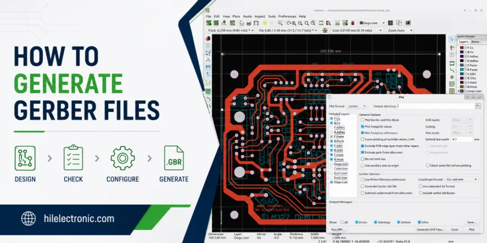
How to Generate Gerber Files for PCB Manufacturing
Figure 1. how to generate Gerber files image for Highleap...
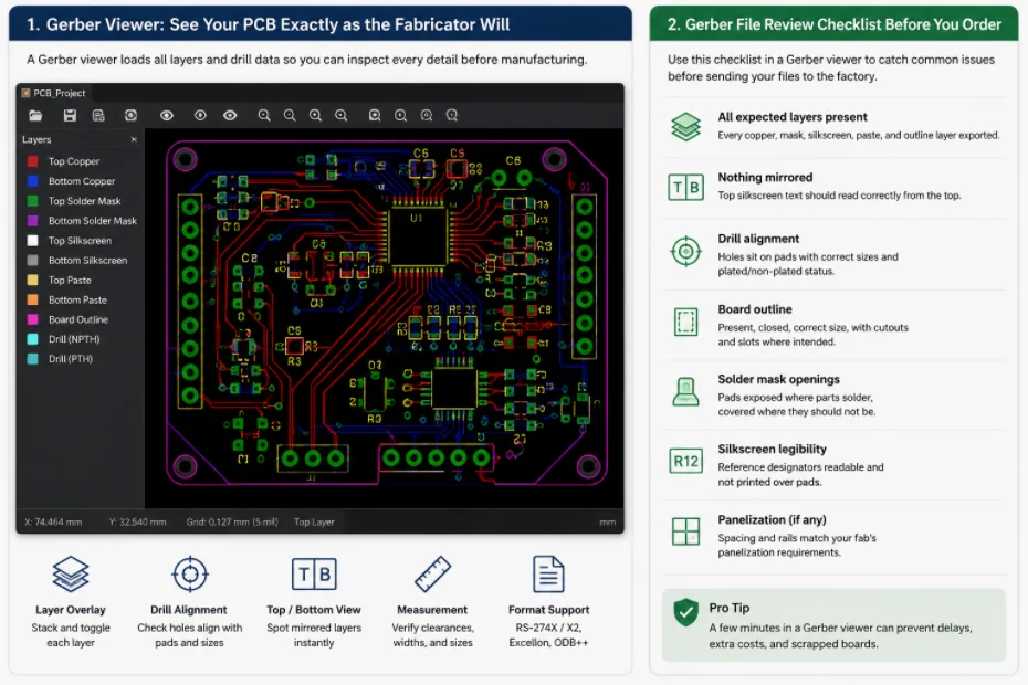
Gerber File Review Checklist: How to Check PCB Files Before You Order
Figure 1. Gerber file review catches missing layers, drill...
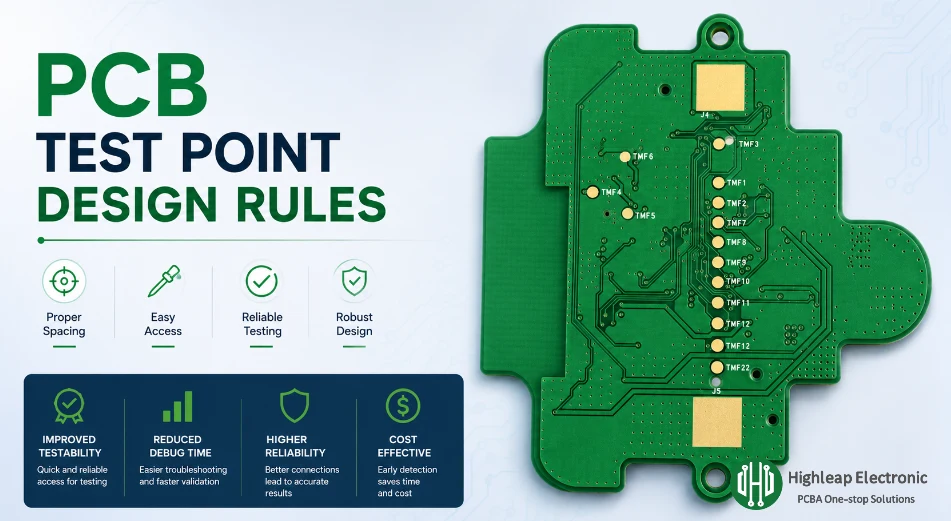
PCB Test Point Design Rules for Debug and ICT
Figure 1. PCB test point design rules help make debugging,...
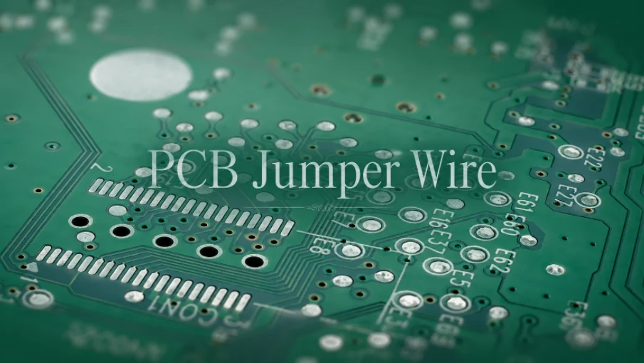
PCB Jumper Wire: Uses, Types, and Design Tips
Figure 1. PCB jumper wires are useful for prototypes and...
How to get a quote for PCBs
Let us run DFM/DFA analysis for you and get back to you with a report.
You can upload your files securely through our website.
We require the following information in order to give you a quote:
-
- Gerber, ODB++, or .pcb, spec.
- BOM list if you require assembly
- Quantity
- Turn time
In addition to PCB manufacturing, we offer a comprehensive range of electronic services, including PCB design, PCBA (Printed Circuit Board Assembly), and turnkey solutions. Whether you need help with prototyping, design verification, component sourcing, or mass production, we provide end-to-end support to ensure your project’s success. For PCBA services, please provide your BOM (Bill of Materials) and any specific assembly instructions. We also offer DFM/DFA analysis to optimize your designs for manufacturability and assembly, ensuring a smooth production process.