
Back to blog
Testing and Validation of Plated Half-Hole PCBs

Plated half-hole PCBs
Through-Hole Technology (THT) in PCB Assembly plays a crucial role in modern electronics manufacturing. It involves mounting components on a PCB by inserting their leads through holes in the board and then soldering them in place on the opposite side. THT offers several advantages, including strong mechanical bonds and the ability to withstand high temperatures and mechanical stress.
In recent years, plated half-hole PCBs have gained popularity due to their ability to provide robust connections while reducing the overall size of the PCB. Plated half-holes are created by drilling holes in the PCB and then plating them with copper to create a solid connection. This technology allows for the use of smaller components and tighter component placement, making it ideal for applications where space is limited.
Plated half-hole PCBs are commonly used in high-density applications where reliability and durability are paramount. They are also used in applications where components need to be mounted on both sides of the PCB, as the plated half-holes provide a secure connection between the two sides.
The Anatomy of Plated Half-Hole PCBs
At the heart of a plated half-hole PCB is the unique castellated hole structure that enables the direct stacking and interconnection of multiple circuit boards. These specialized holes are fabricated by drilling through the PCB substrate and then selectively plating the resulting semi-circular openings with a conductive material, typically copper.
The process of creating plated half-hole PCBs involves several key steps:
- Drilling: The first step in the fabrication process is the precise drilling of holes along the edges of the PCB. The diameter and placement of these holes are critical, as they must align perfectly with the corresponding holes on the mating board to ensure a secure and reliable connection.
- Hole Plating: Once the holes have been drilled, the next step is to plate the inner surfaces of the holes with a conductive material, typically copper. This plating process creates the conductive castellated structures that will serve as the interconnection points between the stacked PCBs.
- Etching and Patterning: With the plated holes in place, the copper traces and pads are then etched and patterned onto the PCB’s surface using standard photolithographic techniques. This step ensures that the electrical signals can be routed from the castellated holes to the desired components and circuitry on the board.
- Solder Mask and Surface Finish: To protect the copper traces and pads, a solder mask is applied to the PCB’s surface. Additionally, a suitable surface finish, such as ENIG (Electroless Nickel Immersion Gold) or HASL (Hot Air Solder Leveling), is applied to the plated holes and pads to enhance solderability and corrosion resistance.
The resulting plated half-hole PCB features a series of concave, conductive pads along the board’s edges, providing a robust and compact interconnection solution. When two or more of these PCBs are stacked and soldered together, the castellated holes form a secure mechanical and electrical connection, enabling the seamless transfer of signals, power, and ground between the boards.
Key Specifications of Plated Half-Hole PCBs
Plated half-hole PCBs are defined by a set of critical specifications that ensure their reliability, performance, and compatibility with various electronic systems. Some of the key specifications include:
1.Hole Diameter and Spacing: The diameter of the plated half-holes is typically in the range of 0.5 mm to 1.0 mm, with a common standard being 0.6 mm. The spacing between the individual half-holes is also a crucial parameter, with a typical spacing of 0.55 mm being common.
2.Hole Plating Thickness: The thickness of the copper plating within the castellated holes is an essential factor, as it directly impacts the electrical and mechanical integrity of the interconnection. A plating thickness of 25-50 microns is generally considered acceptable, ensuring a robust and reliable connection.
3.Surface Finish: The choice of surface finish for the plated half-holes can vary, with options such as ENIG, HASL, or OSP (Organic Solderability Preservative) being common. These finishes enhance the solderability of the pads and provide protection against oxidation and corrosion.
4.Solder Mask Definition: The solder mask, which covers the PCB’s surface, must be carefully defined around the castellated holes to ensure proper wetting and soldering during the assembly process. A well-designed solder mask helps to prevent solder bridging and maintain the integrity of the interconnections.
5.Dimensional Accuracy: The overall dimensional accuracy of the plated half-holes, including their diameter, spacing, and position on the PCB, is crucial. Tight tolerances are required to ensure a precise fit and alignment between the stacked boards, minimizing the risk of electrical shorts or open circuits.
6.PCB Thickness: The thickness of the PCB substrate can also impact the design and performance of the plated half-holes. Thinner PCBs, typically in the range of 0.8 mm to 1.6 mm, are more commonly used for plated half-hole applications, as they allow for more compact and space-efficient stacking of the boards.
7.Material Compatibility: Plated half-hole PCBs can be fabricated using a variety of substrate materials, including FR-4, metal-core, and ceramic-based laminates. The choice of material depends on the specific requirements of the application, such as thermal management, electrical performance, or mechanical robustness.
By adhering to these key specifications, manufacturers can ensure the production of high-quality plated half-hole PCBs that meet the exacting demands of today’s electronic systems.

Applications of Plated Half-Hole PCBs
The unique capabilities of plated half-hole PCBs have made them invaluable in a wide range of applications, where the ability to efficiently stack and interconnect multiple circuit boards is critical. Some of the key industries and applications that rely on this technology include:
- Telecommunications: Plated half-hole PCBs are widely used in the telecommunications industry, where they enable the compact and modular design of equipment such as base stations, routers, and switches. The direct board-to-board connections facilitated by the castellated holes help to minimize signal degradation and improve overall system performance.
- Computing and Electronics: In the computing and electronics sectors, plated half-hole PCBs are employed in the construction of high-density memory modules, CPU sockets, and other space-constrained components. The stacking capability of these boards allows for the efficient packaging of complex electronic systems.
- Automotive Electronics: The automotive industry has embraced plated half-hole PCBs for their use in various electronic control units (ECUs), sensors, and other in-vehicle electronics. The robust mechanical and electrical connections provided by the castellated holes are crucial for withstanding the harsh environments and vibrations encountered in automotive applications.
- Aerospace and Defense: In the aerospace and defense industries, plated half-hole PCBs are utilized in mission-critical systems, such as avionics, guidance and control modules, and portable electronic devices. The reliability and durability of these boards are essential for ensuring the safe and reliable operation of these high-performance systems.
- Industrial Equipment: Plated half-hole PCBs find applications in a variety of industrial equipment, including programmable logic controllers (PLCs), motor drives, and industrial automation systems. The ability to stack and interconnect multiple boards allows for the efficient and compact design of these specialized industrial devices.
- Medical Devices: The compact and reliable nature of plated half-hole PCBs makes them well-suited for use in medical devices, such as patient monitoring equipment, diagnostic instruments, and portable healthcare solutions. The secure board-to-board connections help to ensure the integrity and reliability of these mission-critical medical applications.
- Consumer Electronics: Even in the consumer electronics sector, plated half-hole PCBs are being increasingly adopted for their ability to support the design of smaller, more versatile, and feature-rich products, such as smartphones, wearables, and gaming consoles.
As the demand for more compact, modular, and reliable electronic systems continues to grow, the versatility and performance of plated half-hole PCBs have made them an indispensable technology across a diverse range of industries and applications.
Fabrication Processes and Considerations for Plated Half-Hole PCBs
The production of plated half-hole PCBs requires specialized fabrication processes that differ from those used for conventional rigid or flexible circuit boards. These processes involve several critical steps, each with its own considerations and challenges:
- Drilling: Precise drilling of castellated holes along the board’s edges is essential. Accuracy is crucial to ensure proper alignment and spacing, as deviations can compromise interconnection integrity.
- Hole Plating: After drilling, the inner hole surfaces are plated with a conductive material, usually copper, to create the castellated structures. Plating thickness and quality directly impact electrical and mechanical properties.
- Etching and Patterning: Copper traces and pads are etched and patterned onto the PCB surface using photolithographic techniques. This step routes electrical signals from castellated holes to components.
- Solder Mask and Surface Finish: A solder mask protects copper traces and pads, while surface finishes like ENIG or HASL enhance solderability and corrosion resistance.
- Testing and Inspection: Rigorous testing and inspection ensure quality and reliability, including electrical testing, visual inspection, and AOI to detect defects.
Challenges and Considerations in Plated Half-Hole PCB Fabrication:
- Hole Alignment: Precise alignment of castellated holes is critical to prevent electrical shorts or open circuits, especially when boards are stacked.
- Copper Plating Thickness: Maintaining desired thickness and uniformity is crucial for reliable electrical connections and consistent solder wetting.
- Solder Mask Definition: Careful design and application of the solder mask around castellated holes prevent solder bridging and ensure interconnection integrity.
- Substrate Material Selection: Choice of PCB substrate material impacts fabrication and overall performance. Materials like FR-4, metal-core, or ceramics have different properties and considerations.
- Panel Utilization and Singulation: Optimizing panel use and managing singulation efficiently maximize production efficiency and reduce waste.
Addressing these challenges and maintaining strict quality control can help manufacturers produce high-reliability plated half-hole PCBs that meet the demands of modern electronic systems.
Design Considerations and Tradeoffs
When incorporating plated half-hole PCBs into their designs, engineers must carefully consider a range of factors to ensure optimal performance, reliability, and cost-effectiveness. These design considerations involve balancing the advantages of plated half-hole technology against the potential tradeoffs and limitations.
- Stacking and Interconnection: The primary advantage of plated half-hole PCBs is their ability to enable the stacking and direct interconnection of multiple circuit boards. This capability allows for the creation of compact, modular, and space-efficient electronic assemblies. However, designers must ensure that the castellated holes are precisely aligned and that the mechanical and electrical connections between the stacked boards are secure and reliable.
- Board Thickness and Rigidity: Plated half-hole PCBs are typically thinner than their traditional through-hole counterparts, with board thicknesses commonly ranging from 0.8 mm to 1.6 mm. This reduced thickness can be advantageous for space-constrained applications, but it may also impact the overall rigidity and mechanical robustness of the assembly.
- Signal Integrity and Parasitic Effects: At higher operating frequencies, the castellated holes and the inherent parasitic capacitance and inductance associated with the plated half-hole structure can potentially impact signal integrity and introduce electromagnetic interference (EMI) concerns. Careful design of the trace routing, impedance matching, and grounding strategies is crucial to mitigate these issues.
- Thermal Management: The compact and stacked nature of plated half-hole PCB assemblies can pose challenges in terms of thermal management. The close proximity of components and the limited airflow between the stacked boards can lead to elevated temperatures, which must be addressed through effective heat dissipation strategies, such as the use of heat sinks, thermal vias, or alternative cooling methods.
- Assembly and Rework Considerations: The assembly of plated half-hole PCBs, particularly the soldering of the interconnections between the stacked boards, requires specialized techniques and equipment. Additionally, the rework or replacement of individual boards within a stacked assembly can be more complex and labor-intensive compared to traditional PCB designs.
- Cost Implications: The specialized fabrication processes and assembly requirements associated with plated half-hole PCBs can result in higher manufacturing costs compared to standard rigid or flexible PCBs. However, these increased costs may be offset by the benefits of the technology, such as improved reliability, reduced cabling, and more compact system designs.
By carefully considering these design factors and their associated tradeoffs, engineers can effectively leverage the advantages of plated half-hole PCBs while mitigating the potential limitations to create innovative and high-performance electronic systems.
Engineers usually confirm this topic together with bare board electrical test and through-hole soldering when preparing a reliable PCB or PCBA build.

Plated half-hole PCBs
Advantages and Disadvantages of Half-Hole PCBs:
Half-hole PCBs have gained popularity among experts, offering several advantages and disadvantages that should be carefully considered.
Advantages:
- Simplified Prototyping: Half-hole PCBs are easier to use for prototypes, allowing for quick component changes and modifications.
- Strong Mechanical Links: They provide robust mechanical connections, ensuring reliability in demanding applications.
- Heat Resistance: Half-hole PCBs exhibit good resistance to heat, which is beneficial in high-temperature environments.
- Power Handling Capacity: These PCBs can handle higher power levels compared to traditional PCBs.
Disadvantages:
- Increased Board Costs: The process of creating half-holes can increase the overall cost of the PCB due to additional manufacturing steps.
- Larger Board Space Requirement: Half-hole PCBs occupy more board space, limiting the available area for other components.
- Complex Assembly: Assembling half-hole PCBs can be more challenging and time-consuming compared to traditional PCBs.
- Higher Parasitic Effects: At high frequencies, half-hole PCBs may exhibit higher parasitic effects, impacting performance in applications requiring high-frequency operation.
Despite these drawbacks, half-hole PCBs are preferred in applications such as automotive, aerospace, and military electronics, where robustness and reliability are paramount. Additionally, the technology is well-suited for prototyping and experimentation, allowing for rapid iteration and design changes. As technology advances, the trend towards smaller and more efficient PCBs continues, with half-hole mounting technology playing a crucial role in achieving these goals.
Reliability and Testing of Plated Half-Hole PCBs
Ensuring the long-term reliability and performance of plated half-hole PCBs is of paramount importance, as these interconnection solutions are often deployed in mission-critical applications across various industries. To validate the robustness and durability of plated half-hole PCBs, a comprehensive suite of reliability tests must be conducted, focusing on the unique failure modes and stress factors associated with this technology.
Key Reliability Tests for Plated Half-Hole PCBs:
- Mechanical Integrity Tests: These tests evaluate the mechanical strength and integrity of the plated half-hole interconnections, including their resistance to shear, tensile, and bending stresses. This helps to ensure the reliability of the stacked board assembly during installation, handling, and in-service operations.
- Thermal Cycling and Shock Tests: Thermal cycling and shock tests subject the plated half-hole PCBs to extreme temperature fluctuations, simulating the environmental conditions they may encounter during their lifetime. These tests assess the ability of the interconnections to withstand the resulting thermal expansion and contraction without failure.
- Vibration and Shock Tests: Vibration and shock tests are performed to evaluate the resilience of the plated half-hole PCBs to the dynamic stresses and impacts they may experience in various applications, such as automotive, aerospace, or industrial environments.
- Corrosion and Environmental Tests: Corrosion and environmental tests, including exposure to humidity, salt spray, and other corrosive agents, are conducted to assess the suitability of the plated half-hole PCBs for use in harsh operating conditions.
- Electrical Performance Tests: Electrical performance tests, such as impedance measurements, crosstalk analysis, and high-frequency signal integrity evaluations, are performed to ensure that the plated half-hole interconnections do not adversely impact the electrical characteristics of the circuit.
- Accelerated Aging Tests: Accelerated aging tests, which subject the plated half-hole PCBs to elevated temperature and humidity conditions for extended periods, help to predict the long-term reliability and service life of the interconnections.
By conducting a comprehensive suite of reliability tests, manufacturers and designers can validate the performance and durability of plated half-hole PCBs, ensuring that they meet the stringent requirements of their target applications.
Conclusion
Plated half-hole PCBs have revolutionized the way electronic systems are designed and assembled, offering a unique combination of compactness, modularity, and reliability. As electronic devices become increasingly complex and space-constrained, the versatility and performance of plated half-hole PCBs make them an indispensable technology across a wide range of industries and applications.

Related Articles
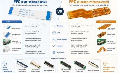
FFC vs FPC: Cable, Circuit, Connector Guide
Understand the difference between FFC and FPC interconnects, where each fits best, and how to choose compatible connectors for reliable assembly.
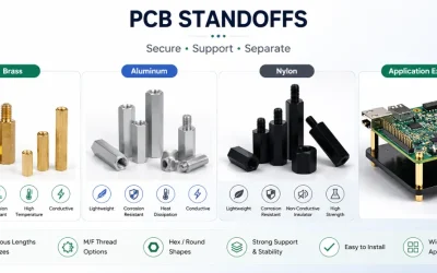
PCB Standoffs and Spacers Selection Guide
Choose PCB standoffs and spacers by material, thread size, height, and grounding needs to protect boards and simplify enclosure assembly.
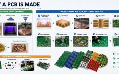
How a PCB Is Made: Fabrication Process Guide
See how a PCB is made, from home etching to professional fabrication, and learn when to move to factory processes for accuracy, yield, and assembly.