
Back to blog
Your Reliable PCB Gold Finger Manufacturer in China
PCB gold fingers serve as essential components in the realm of contemporary electronics. These gold-plated connectors, typically found at the board edges of printed circuit boards (PCBs), facilitate critical connections and power distribution within electronic devices. In this extensive guide, we will explore different facets of PCB gold fingers, encompassing their production processes, applications, design considerations, and the significance of selecting a trustworthy manufacturer.

What Are PCB Gold Fingers?
PCB gold fingers, commonly referred to as edge connectors, are rows of square pad connectors that feature a layer of gold plating. These connectors are strategically positioned at regular intervals along the edges of printed circuit boards (PCBs). Their primary purpose is to establish a reliable interface between various PCBs or between a PCB and its corresponding slot. By facilitating the smooth transmission of signals and power, PCB gold fingers play a crucial role in enabling seamless connectivity and optimal performance of electronic devices. Their presence is essential, making them a fundamental and integral component in the world of modern electronics.
Applications of PCB Gold Fingers
The importance of PCB gold fingers extends to a wide range of electronic devices, including but not limited to:
Computers: PCB gold fingers facilitate the connection of expansion cards, memory modules, and other peripherals to the motherboard.
Smartphones: These connectors play a crucial role in connecting various internal components within smartphones, ensuring smooth functionality.
Televisions: In modern high-definition TVs, PCB gold fingers are used to connect display panels, processors, and other critical components.
Laptops: Similar to desktop computers, laptops utilize gold fingers to establish connections between internal components, such as RAM modules and graphics cards.
Memory Cards: Memory card readers and slots often feature gold-plated connectors for fast and reliable data transfer.
Industrial Electronics: PCB gold fingers are integral to industrial automation systems, medical devices, and other specialized equipment that rely on high-speed data transmission and power distribution.
Automotive Electronics: Modern vehicles incorporate advanced electronics, and PCB gold fingers are used in components like airbag modules, infotainment systems, and engine control units.
PCB Gold Finger Plating Thickness
The thickness of gold plating on PCB gold fingers is a critical factor that affects their performance and durability. Two common types of gold plating used are:
- Electroplating Nickel Gold: This method allows for gold thickness ranging from 3 to 50 microns. It is suitable for applications that require frequent insertion and removal or components subjected to mechanical friction. Gold’s excellent conductivity, oxidation resistance, and wear resistance make it an ideal choice.
- Immersion Gold (ENIG): Immersion gold typically has a gold thickness of 1 to 3 microns. It is preferred for high-precision PCBs with fine-pitch components, such as ICs and BGAs. ENIG provides superior conductivity, flatness, and solderability. It is a cost-effective alternative to electroplated gold.
PCB Gold Finger Details Processing
To ensure the reliability and functionality of PCB gold fingers, specific processing steps must be followed:
- Beveling: The edges of PCB gold fingers are beveled at angles typically ranging from 20 to 45 degrees. Beveling facilitates smooth insertion into corresponding slots, ensuring a secure fit.
- Solder Mask Window: A solder mask window is created to expose the gold finger’s pad while keeping the surrounding area covered. This allows for proper soldering and electrical contact.
- Distance from Other Components: To prevent interference, it’s crucial to maintain a minimum distance of 0.5 to 0.7 mm between the gold finger and the PCB’s periphery. Avoid placing through-holes, solder masks, or screen printing near the gold finger.
- Copper Avoidance: The gold finger’s surface should not be covered with copper, as this can impact its performance and reliability.
- Inner Layer Copper Cutting: All layers of the inner layer of the gold finger need to have copper cut, typically with a width of 3 mm or more.
let’s incorporate the additional details into the processing and manufacturing of PCB gold fingers:
- Drill Hole Placement Away from Gold Finger Area: It’s important to strategically place drill holes at a distance from the gold finger area. This prevents any accidental drilling through the gold fingers, ensuring their integrity and functionality.
- Caution When Creating Dummy Fingers: When creating dummy fingers (imitation gold fingers), it’s essential to be cautious and ensure that they do not extend into other units or sections of the PCB. This prevents unintended connections or interference between different parts of the PCB.
- Attention to Detail When Creating Peelable Finger Leads: In cases where peelable finger leads are needed, thorough inspection is necessary to ensure that no finger leads are accidentally omitted during the manufacturing process. Properly designed peelable finger leads should function as intended when they are later removed.
- Maintaining Proper Spacing During Panelization: When panelizing multiple PCBs, adhering to industry standards and guidelines for maintaining appropriate spacing between individual PCBs is crucial. This practice prevents crowding or overlapping, which could affect the performance or reliability of the gold fingers.
- Adhering to Standard Practices: Following industry-standard practices for PCB gold finger processing remains critical. Adherence to established guidelines and specifications is essential for producing gold fingers that meet the required standards for reliability, functionality, and performance.
Incorporating these additional steps into the processing and manufacturing of PCB gold fingers enhances the quality and reliability of the connectors. These measures help prevent interference, ensure proper electrical connections, and contribute to the production of high-quality PCBs with gold fingers.
Attentions for panelized with Gold Finger PCB
- In a panel, you can design up to 6 rows of gold fingers, which means you can simultaneously electroplate a maximum of 3 rows of fingers when electroplating from one side. Mixing horizontal and vertical arrangements is not allowed.
- After panelization, each row of gold fingers must meet the following criteria simultaneously: it must be ≤8 inches from one side parallel to it, and it must be ≥8 inches from the other side of the board.
- For gold finger orders with size restrictions resulting in low panel utilization, the method of cutting boards can be used to plate gold fingers. The spacing between the upper and lower parts of the two-unit boards must be ≥5mm. ERP should add a cutting board process before plating gold fingers, providing instructions on where to cut boards to improve utilization.
- The distance between the base of adjacent two rows of gold fingers must be ≤30mm, and all gold fingers should be plated at once.
- When the distance between the base of adjacent two rows of gold fingers is >30mm, the distance between the tops of the adjacent two rows of gold fingers must be >20mm.
- The width of the gold finger plating lead in the panel is 40 mils, and it must extend to the copper skin at the edge of the board.
- Design requirements for panels with multiple gold finger arrays: Gold fingers should preferably be designed towards the center of the board. If both sides of the board have gold fingers, with one side being larger than the other, design the larger gold fingers towards the center. If both sides have equally sized gold fingers, consider changing the panel arrangement or placing the gold fingers on the wider side of the board. (Single and multiple panel arrangements are specific to APNL panelization.)
PCB Gold Finger Beveling

Beveling plays a crucial role in the manufacturing process of PCB gold fingers. It involves shaping and cutting the edges of the connectors to create a sloping side. The purpose of beveling is to facilitate smooth and easy insertion of the gold fingers into their corresponding slots, thereby enhancing the overall reliability of the connections.
The beveling angles for PCB gold fingers typically range from 20 to 45 degrees, although other angles can be employed based on specific requirements. The chosen beveling angle should strike a balance between ensuring proper alignment and secure insertion of the gold fingers while considering the space constraints and design considerations of the PCB.
By implementing appropriate beveling techniques, manufacturers ensure that the gold fingers are precisely shaped and finished, allowing for efficient and reliable connections within electronic devices.
PCB Gold Finger Repair
In certain instances, PCB gold fingers may require repair, particularly when they become damaged due to solder splashes, pitting, or scratches. PCB gold finger repair is a specialized process that necessitates the expertise of skilled technicians. The repair procedure typically involves the following steps:
- Solder Removal: Excess solder is carefully removed using a wicking technique. If necessary, additional mechanical and chemical stripping methods may be employed.
- Buffing: Scratched or pitted areas on the gold fingers may undergo a buffing process to smoothen the surface and restore its integrity.
- Replating: In cases where the gold plating is significantly damaged, the affected gold fingers can be replated. This involves depositing a new layer of gold onto the damaged areas to restore their functionality.
Repairing PCB gold fingers requires a combination of patience, dexterity, and specialized equipment, making it a task best suited for experienced technicians who possess the necessary skills and expertise in this domain.
Advantages of PCB Gold Finger

PCB gold fingers offer several advantages that make them a preferred choice in electronic devices:
- Cost-Effective: PCB gold fingers are a cost-effective solution for reliable connections in electronic devices.
- Re-Workable: Damaged or contaminated gold fingers can be repaired or replaced, extending their lifespan.
- Excellent Conductivity: Gold plating ensures high conductivity, facilitating efficient signal transmission.
- Oxidation Resistance: Gold is resistant to oxidation, ensuring long-term reliability.
- Heat Resistance: PCB gold fingers can tolerate high temperatures without degrading.
- Corrosion Resistance: They are resistant to corrosion, making them suitable for various environments.
- Flexibility: PCB gold fingers can fit into different shapes and configurations.
- Long Shelf Life: They have a long shelf life and offer durability in various applications.
- Lead-Free: PCB gold fingers are lead-free, aligning with modern environmental standards.
PCB Gold Finger Thickness
The thickness of PCB gold fingers is a critical factor that significantly impacts their performance and conductivity. It is essential to select an appropriate gold thickness to ensure optimal functionality and reliability. The recommended gold thickness for PCB gold fingers typically falls within the range of 2 to 5 micro inches.
Standard thickness options for PCB gold fingers include 0.031, 0.062, 0.093, and 0.0125 micro inches. The specific choice of thickness depends on various factors, such as the design requirements of the PCB, the intended application, and the desired electrical performance.
Thicker gold plating offers improved durability and longer lifespan, providing enhanced resistance to wear and corrosion. Thinner gold plating, on the other hand, may be suitable for applications with space constraints or where cost considerations are a significant factor.
When determining the appropriate gold finger thickness for a PCB, it is crucial to consider the specific requirements of the design, the expected electrical performance, and any relevant industry standards or customer specifications. By selecting the right gold thickness, manufacturers can ensure reliable and efficient connectivity within electronic devices.
Impact of PCB Gold Finger
The utilization of PCB gold fingers has had a significant impact on the electronics industry, revolutionizing the way electronic devices are designed and operated. The following are some key impacts of PCB gold fingers:
Enhanced Connectivity: PCB gold fingers provide a reliable and efficient means of interconnecting various components within electronic devices. Their precise design and gold plating ensure high conductivity and low resistance, enabling fast and seamless communication between different parts of the circuit.
Improved Device Performance: The use of PCB gold fingers facilitates high-speed signal transmission and efficient power distribution. This results in improved device performance, reduced signal loss, and enhanced overall functionality. Through the reliable connections enabled by gold fingers, electronic devices can operate at their full potential.
Miniaturization and Space Efficiency: PCB gold fingers allow for compact and space-efficient designs. The precise placement and small footprint of these connectors enable the creation of smaller and more lightweight electronic devices. This has led to advancements in areas such as mobile devices, wearables, and IoT devices, where compactness and portability are essential.
Reliability and Durability: PCB gold fingers are designed to withstand repeated insertions and removals, ensuring long-term reliability and durability. The gold plating provides excellent corrosion resistance, protecting the connectors from oxidation and maintaining their performance over time.
Advancement of Industries: The impact of PCB gold fingers extends beyond consumer electronics. They have played a vital role in advancing industries such as telecommunications, automotive, aerospace, medical devices, and more. These connectors enable the development of sophisticated electronic systems and facilitate seamless integration of complex components.
In summary, PCB gold fingers have had a profound impact on the electronics industry, contributing to improved connectivity, device performance, miniaturization, reliability, and advancements in various sectors. Their role as essential connectors continues to shape the technological landscape and drive innovation in electronic devices.
PCB Gold Finger Connector

A PCB gold finger connector, also referred to as an edge connector, is a vital component that facilitates the interconnection between PCBs or between a PCB and its corresponding slot in a device. These connectors are composed of metallic tracks that establish electrical connections when inserted into slots.
Edge connectors are ubiquitous in various electronic devices and are essential for their proper operation. They offer several advantages, including:
Durability: PCB gold finger connectors are designed to withstand repeated insertions and removals, ensuring long-term reliability and durability.
Simplicity: These connectors have a straightforward design, making them easy to manufacture, install, and replace if necessary.
Cost-effectiveness: Edge connectors are often cost-effective in comparison to other complex interconnect solutions. Their simplicity in design and production contributes to their affordability.
Efficiency: PCB gold finger connectors provide efficient electrical connections, enabling fast and reliable signal transmission and power distribution between PCBs or between a PCB and its corresponding slot.
Due to their durability, simplicity, cost-effectiveness, and efficiency, edge connectors are widely used in the electronics industry. They are commonly found in devices such as computer motherboards, memory modules, expansion cards, connectors for display panels, and more. The versatility and reliability of PCB gold finger connectors make them a popular choice for achieving seamless connectivity in electronic devices.
Why Gold Plating Is Necessary for PCB Gold Finger
Gold plating is necessary for PCB gold fingers due to several key advantages it offers:
- Prevents Damage: Gold plating protects PCB gold fingers from damage caused by frequent insertion and removal.
- Enhances Durability: Gold plating increases the durability of PCB gold fingers, extending their lifespan.
- Low Contact Resistance: Gold’s excellent conductivity ensures low contact resistance, maintaining reliable electrical connections.
- Oxidation Resistance: Gold’s resistance to oxidation ensures that PCB gold fingers maintain their functionality over time.
- Improved Heat Resistance: Gold plating enhances the heat resistance of PCB gold fingers, making them suitable for high-temperature applications.
- Corrosion Resistance: Gold-plated connectors are resistant to corrosion, making them ideal for various environments.
Choosing a PCB Gold Finger Manufacturer
Selecting a reputable PCB gold finger manufacturer is crucial to ensure the quality and reliability of your electronic devices. One such manufacturer is Highleap, a company with over 15 years of experience in PCB gold finger manufacturing. Highleap offers a range of benefits:
Comprehensive Solutions: Highleap can provide PCB gold finger solutions for various PCB types, from single-sided to 40-layer boards, including rigid, flexible, and rigid-flex PCBs.
In-House Processes: To maintain quality control, Highleap performs all gold finger processes in-house, ensuring the highest standards of quality.
Customization: Highleap offers flexibility in gold thickness, ranging from 2 to 50 microns, allowing customers to tailor their requirements.
No Minimum Order Quantity: Highleap accommodates orders of any size, with no minimum quantity requirements.
Quality Assurance: All PCB gold fingers undergo 100% E-test and AOI inspection to guarantee quality and reliability.
Choosing Highleap as your PCB gold finger manufacturer ensures that you receive high-quality products, comprehensive solutions, and excellent customer support. Their extensive experience and commitment to quality make them a reliable partner for your PCB gold finger needs.
Conclusion
PCB gold fingers are indispensable connectors in modern electronics, enabling the seamless flow of signals and power between devices. Their reliability, durability, and versatility make them a preferred choice in various applications, from consumer electronics to industrial automation. Choosing a reputable manufacturer like Highleap ensures that you receive high-quality PCB gold fingers that meet your specific requirements. As technology continues to advance, PCB gold fingers will remain a vital component in the world of electronics, contributing to the efficiency and functionality of electronic devices. With Highleap’s expertise and commitment to quality, you can trust in the performance and reliability of their PCB gold fingers for your electronic projects.
PCB & PCBA Quick Quote
Related Articles
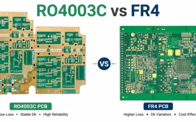
RO4003C vs FR4 PCB Electrical and Thermal Performance
Compare RO4003C vs FR4 PCBs for high frequency and automotive radar learning dielectric loss impedance stability thermal performance and material selection

Rogers PCB Automotive Radar Design and Material Selection
Explore Rogers PCB automotive radar stackup, including RO3003, RO4835, and RO4003C materials, hybrid FR4 layers, and high-frequency design for reliable RF performance.
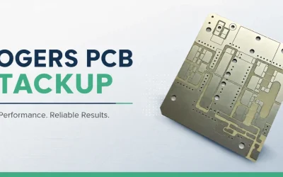
Rogers PCB Stackup Layer and Material Selection
This guide covers Rogers PCB Stackup configurations, RO4000 cores, FR4 layers, and prepreg selection to optimize RF performance and reliability.