
Back to blog
PCB Manufacturing Efficiency with CAM350

CAM350
The CAM350 tool serves as a pre-processing and design verification system tailored for design engineers or process engineers who transmit designs to PCB manufacturers in formats such as Gerber, ODB++, or IPC-2581. It is often used alongside BluePrint design documentation preparation software but can also function as a standalone product.
The system boasts an extensive array of design checks focusing on Design For Manufacturing (DFM), Design For Assembly (DFA), and Design For Test (DFT) to identify errors, non-technological areas, bottlenecks, and defects. It then rectifies these issues within the original PCB project. Additionally, certain corrections can be directly applied to Gerber files, streamlining the design verification and correction process.
CAM350 Basic Steps to Create CAM Data Summary
CAM350 is a crucial tool in the PCB manufacturing process, enabling the creation of accurate CAM data for efficient production. Let’s delve into the detailed steps involved in creating CAM data using CAM350.
- File Import and Verification
- Start by importing the file (File–>Import–>Autoimport) and verify that the data is complete.
- Align the layers (Edit–>Layers–>Align) to ensure accurate representation.
- Set the origin (Edit–>Change–>Origin –>Datum Coordinate) for precise positioning.
- Arrange layers in the desired order (Edit–>Layers–>Reorder) and delete any unused layers (Edit–>Layers–>Reorder).
- Drilling Process
- If the drilling file is not provided, create drill data using aperture hole conversion to Flash (Utilities–> Draw–> Custom, Utilities–> Draw–> Flash–> Interactive) and then to drill (Utilities–>Gerber to Drill).
- Check minimum drilling hole size, hole-to-hole spacing (Analysis–>Check Drill), and minimum distance between hole edge and routing edge (Info–>Measure–>Object-Object) to ensure process capability.
- Line Processing
- Measure minimum wire diameter and spacing (Analysis–>DRC) to meet process capability.
- Adjust circuit PAD offset relative to drill hole if needed (Edit–>Layers. –>Snap Pad to Drill) or vice versa (Edit–>Layers–>Snap Drill to Pad).
- Verify that circuit PAD rings are large enough (Analysis–>DRC) and check edge clearances for manufacturing requirements.
- Ensure cancellation of line PADs for NPTH holes (Edit–>Delete).
- Verify spacing between circuit and line, line and PAD, and PADs meet manufacturing requirements.
- Solder Mask Alignment
- Check alignment between solder mask and line PAD (Analysis–>DRC).
- Verify solder mask and line spacing, solder mask and line PAD spacing.
- Ensure minimum solder mask width and specific solder mask for NPTH (Add–>Flash).
- Character Processing
- Verify character line width (Info–>Report–>Dcode), height, hollow diameter, and spacing with line PAD.
- Check distances between characters and routing edge, slot hole, and PTH (no tin) for manufacturing requirements.
- Add UL MARK and DATE CODE marks as required by the customer, ensuring they are not added to restricted areas.
- Sets and Working Side Processing
- Duplicate sets according to specifications (Edit–>Copy) and add working side information.
- Include AI holes, position holes, optical points, and material numbers as needed.
- Add V-CUT corners and other required elements.
- Panelization and Artwork Borders
- Panelize according to specified panel type and create artwork borders according to production specifications.
- Layers
- Use Tables–>Composites to add a Composites Name, set the polarity of the screen’s back (positive and negative), and manage layers.
- Output Drilling and Light Drawing Data
- Record minimum line diameter, line spacing, and copper area of the original sheet and worksheet.
- Print aperture hole position and drill report table.
- Output drill data (File–>Export–>Drill Data) and light drawing data (File–>Export–>Composites) in the specified formats.
By following these detailed steps, you can create accurate and efficient CAM data using CAM350, ensuring a smooth manufacturing process for PCBs.
For a more complete production review, use this article alongside production PCB manufacturing and electronic component sourcing when checking stackup, assembly, or test requirements.
How to panelize PCBs with CAM350
CAM350 is a software tool widely used by electronic engineers to check designs and panelize PCBs for SMT production, reducing PCB costs. Highleap Electronic offers PCB fabrication services to help users lower their PCB costs. Here’s a step-by-step tutorial on how to panelize PCBs using CAM350 to make designs more effective and cheaper:
Opening Gerber Files with CAM350
- Open Gerber Files: Go to File -> Import -> Autoimport.
- Choose Directory: Select the directory containing your Gerber files.
- Exclude Drill Layer: Do not select the drill layer during import.
- Finish Import: Press the Finish button to complete the import.
- Import Drill Layer: Go to File -> Import -> Drill Data, select the drill layer file, choose “All Files,” and double-click the drill layer file. Then, select Leading and press OK.
Saving as PCBname.cam File
- Panelize PCBs: Press File -> New, then click File -> Open and open PCBname.CAM.
- Merge Files: Press File -> Merge, select the file you want to panelize, and open it.
- Confirmation: Press OK to confirm.
- Placement: Right-click to place the file anywhere on the board.
- Move Files: Press Edit -> Move to move the next Gerber files to where you want to place them.
- Explode Layers: Press Edit -> Change -> Explode -> All.
- Confirmation: Right-click the whiteboard and press Yes.
- Merge Layers: Double-click the GBO layer (example), press Select All, then press Move To Layer.
Exporting Gerber Data
- Export Gerber Data: Press File -> Export -> Gerber Data.
- Select Export Path: Choose where to export and change the filenames as required, then press OK.
- Export Drill Data: Press File -> Export -> Drill Data, change the drill layer filename, and press OK.
After exporting, open the exported Gerber file (File -> New) to verify its correctness. Ensure the following PCB layers are included:
- Top Copper (GTL)
- Bottom Copper (GBL)
- Top Silkscreen (GTO)
- Bottom Silkscreen (GBO)
- Top Solder Mask (GTS)
- Bottom Solder Mask (GBS)
- Drills (TXT)
By following these steps, you can effectively panelize PCBs using CAM350, reducing costs and improving efficiency in PCB production.
Advanced Materials and Manufacturing Techniques
CAM350 offers several advantages that streamline the PCB manufacturing process. It reduces redundancy by minimizing repeated design efforts, thereby reducing waste and lowering costs. Additionally, CAM350 enhances the manufacturability of PCB designs, ensuring they can be efficiently produced. This leads to faster production cycles, as the tool streamlines the design-to-production process, improving overall efficiency.
Moreover, CAM350 automates various design processes, resulting in optimized designs and increased efficiency. It also improves quality and database management, helping to maintain high standards and efficiently manage design databases. Overall, CAM350 contributes to efficient mass production of bare boards, further enhancing production efficiency.
Main Functions of CAM350
- Format Support: Supports multiple input/output formats (CAD data, ODB++, Gerber, IPC-356, Excellon, DXF, Sieb and Myers) and provides two-way AutoCAD and DXF support.
- Design Rule Inspection: Includes spacing, loop lines, copper foil area calculation, and netlist comparison for design optimization.
- NC Editor: Basic through-hole editing functions, drilling tool definition, milling path, and tool lifting point management.
- Fast Boarding: Allows PCB array creation to meet production requirements and generates accurate manufacturing process requirement lists.
- Interactivity and Error Detection: Supports interactive Cross-probe and highlights errors in CAD tools (Allegro and PADS) for quick correction.
- Netlist Comparison: Enhanced netlist comparison function with graphical error representation for easier error detection and correction.
- Batch Rule Check: Allows users to define and execute a series of design rule checks (DRC), design for fabrication (DFF), and netlist comparisons for efficient verification.
CAM350’s comprehensive features and functionalities make it a valuable tool for PCB manufacturers, helping them address design challenges and optimize the production process.

Recommended Posts

PCB Current Calculator: Sizing Trace Width and Vias with the IPC-2221 Formula
Figure 1. Pcb Current Calculator reference image for PCB...

Microphone PCB Design: How the Board Itself Shapes Your Audio Quality
Figure 1. Microphone Pcb reference image for PCB...
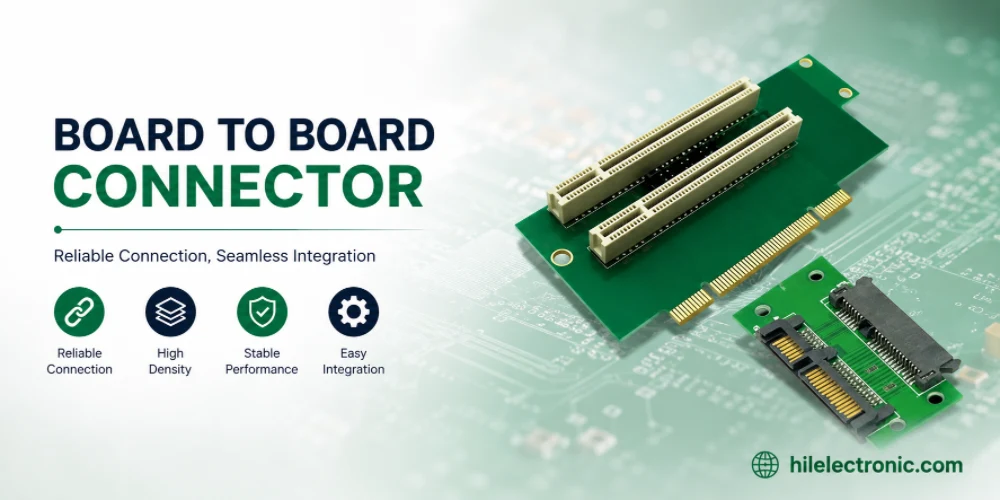
Board-to-Board Connector: Types, Specifications, and How to Select One
Figure 1. Board To Board Connector reference image for PCB...
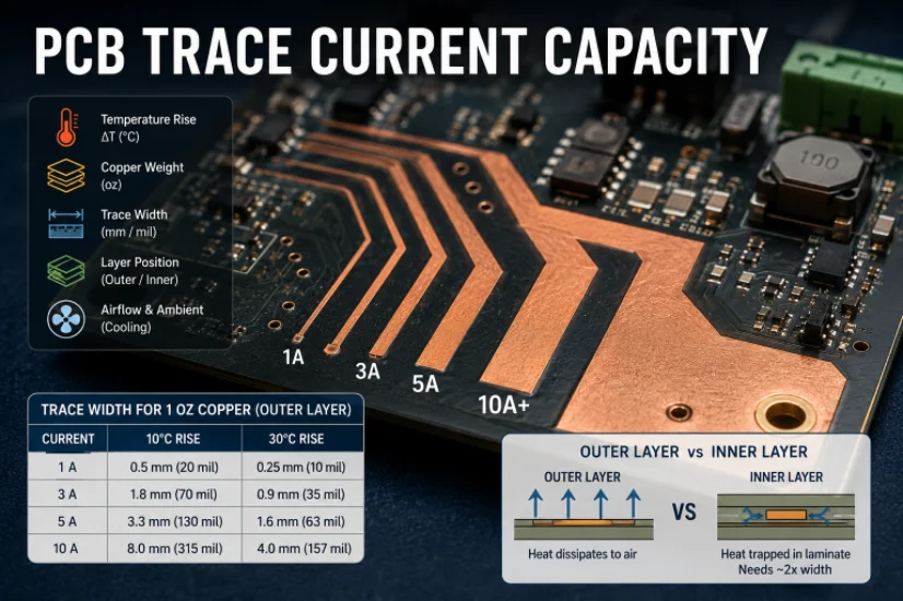
PCB Trace Width Calculator: How to Size Traces for Current, Voltage Drop, and Impedance
Figure 1. A PCB trace width calculator is a starting point...