
Back to blog
Optimizing PCB Profiling Techniques for Enhanced Manufacturing
Introduction
PCBs serve as the backbone of modern electronics, enabling the functionality of countless devices we use in our daily lives. The process of manufacturing PCBs involves a series of intricate steps, with PCB profiling, also known as routing, standing out as a critical stage. Profiling determines the quality of PCB edges and the accuracy of their final shapes. For PCB manufacturers, the choice of profiling technique plays a pivotal role in achieving a balance between cost, speed, and quality.
Highleap, a leading PCB manufacturer based in China, has consistently delivered high-quality PCBs by leveraging innovative profiling methods. In this comprehensive article, we delve into the world of PCB profiling, exploring the four most prevalent techniques in the industry: laser cutting, punching, router cutting, and V-cutting. We will dissect each method’s working principles, delve into their advantages and limitations, and analyze their impact on PCB quality. Furthermore, we will discuss strategies for PCB manufacturers to select the most suitable profiling method tailored to their specific production requirements and volumes.
This article aims to provide in-depth insights, valuable background knowledge, and data-driven analysis for professionals involved in PCB manufacturing. Whether you are a newcomer to PCB profiling or an industry veteran looking to optimize your processes, this article offers a wealth of information and practical guidance to enhance your operations.
Common PCB Profiling Methods
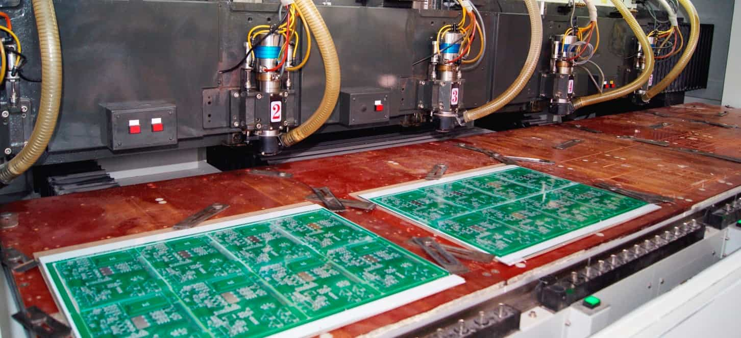
In the world of PCB manufacturing, several profiling techniques are commonly employed, each carrying its own set of merits and demerits. The choice of profiling method is a critical decision that can significantly impact productivity, cost-efficiency, and the overall quality of the final PCB. The four primary PCB profiling methods we will explore are laser cutting, punching, router cutting, and V-cutting.
Laser Cutting

Laser cutting stands out as one of the most precise and advanced PCB profiling techniques available. It harnesses the power of a high-energy laser beam, often operating in the ultraviolet (UV) or carbon dioxide (CO2) wavelength range, to vaporize material along the designated cutting path. The laser’s focused beam ensures a narrow cut width, cleanly ablating the material without inducing excessive heat damage.
In comparison to conventional mechanical cutting tools, laser cutting offers unparalleled cut quality and precision. The cut edges are remarkably smooth, devoid of burrs or roughness. Laser cutting excels at handling intricate patterns and sharp corners, achieving tolerances as tight as ±0.001 inches.
The non-contact nature of laser cutting eliminates concerns related to tool wear and deformation, ensuring consistency in the cutting process. Additionally, the cutting speed can be readily adjusted by controlling laser power and repetition rate. Laser profiling generates minimal dust and waste, further enhancing its appeal.
However, laser cutting demands a substantial initial investment in terms of acquiring the laser source, motion systems, optics, and operating software. Its cutting speed, while impressive, may be slower when compared to mechanical tools. Operating costs, particularly with regard to energy consumption and gas usage, tend to be higher.
In summary, laser cutting excels in delivering top-tier profiling quality and precision. This method finds its niche in the production of high-end PCBs, particularly flexible and rigid-flex PCBs, where edge finish and dimensional accuracy are paramount. The non-contact nature of laser cutting ensures clean cuts across a wide spectrum of materials. While laser profiling may not be the most cost-effective solution for high-volume production, it offers an attractive proposition for low to medium-volume PCB manufacturing.
Punching
Punching relies on a mechanical punching head to execute the profiling process. The punching head features a sharp punch that descends to penetrate the PCB material, effectively creating a hole around the PCB profile edge as it progresses.
One of the defining characteristics of punching is its exceptional speed. Punching is capable of profiling at astonishing rates, often exceeding 10,000 holes per minute. This method’s efficiency extends to internal cutouts and void areas, making it well-suited for automation in linear configurations.
However, punching fails to deliver the clean-cut edges that laser cutting achieves. Micro-cracks may form around the perimeter of punched holes, potentially affecting the structural integrity of the PCB. Additionally, the process generates debris, necessitating supplementary cleaning steps.
Punching also exhibits lower accuracy, typically within the range of ±0.002 inches, primarily due to potential tool wear and deformation over time. To mitigate these issues, specialized hard tools constructed from materials such as carbide or diamond are employed, extending the tool’s operational life.
In essence, punching shines when speed and throughput are the primary considerations. This method’s suitability is particularly evident in high-volume PCB production, leveraging its automation capabilities. Although the pursuit of exceptional edge finish may necessitate exploring alternative methods, the advantages of cost efficiency and rapid production often outweigh this drawback for many PCB manufacturers.
Router Cutting
Router cutting employs a rotating cutting tool equipped with a carbide tip to shape the edges of the PCB. The high-speed spindle spins the router bit, often reaching speeds of up to 40,000 revolutions per minute (rpm), allowing for efficient material removal. The PCB is securely fastened to a movable table that follows a predetermined tool path.
Router profiling achieves a commendable level of cut quality, delivering smooth edges. The rigid and precise router bit maintains tolerances typically within the range of ±0.003-0.005 inches. Routers demonstrate impressive versatility, proficiently executing both straight and beveled cuts.
One of router cutting’s notable advantages is its swift setup, rendering it highly efficient for small to medium batch sizes. The ability to automate tool changes facilitates the profiling of complex internal cutouts. Routers boast high uptime and are relatively cost-effective machines.
However, it is important to note that routers generate more debris and noise in comparison to laser and punching methods. The router bits necessitate frequent sharpening or replacement when they wear down. Additionally, routers exhibit limitations concerning cut radius and contour complexity.
In summary, router cutting offers a balanced combination of cut quality, flexibility, and cost-effectiveness, rendering it suitable for a wide spectrum of PCB profiling applications. It excels in handling a diverse array of materials and proves productive, seamlessly scaling from prototyping to high-volume production.
V-Cut
V-cutting, characterized by its simplicity, represents a mechanical profiling method that employs a V-shaped cutting tool tipped at a 45-degree angle. The sharp tip of the V-Cut blade simultaneously penetrates the top and bottom surfaces of the PCB, meeting at the center.
V-Cut’s primary advantage lies in its cost-effectiveness and speed relative to other methods. This technique requires minimal setup and can execute cuts rapidly, rendering it particularly favorable for high-volume PCB batch production.
However, V-Cut’s Achilles’ heel is its relatively lower cut quality. The resulting edges are often jagged and uneven, potentially featuring burrs. The kerf width, the material removed during the cutting process, tends to be larger, leading to higher material wastage. Additionally, without proper blade clearances, copper smearing can become a significant issue.
While innovations in V-Cut technology, such as multi-tooth blades, have improved cut quality, the method remains less precise when compared to routing, punching, and laser techniques. Typical tolerances for V-Cut profiling range from ±0.004-0.008 inches. Moreover, V-Cut is limited in its ability to execute only straight-line cuts and basic geometries.
In summary, V-Cut presents an economical profiling option, ideally suited for straightforward board shapes where edge finish holds less significance. The method’s swift processing speeds make it a valuable asset in high-volume PCB production. However, it is important to acknowledge that cut quality is sacrificed in favor of efficiency when compared to alternative methods.
How To Choose The Right PCB Profiling Method
Having delved into the intricacies of the four major PCB profiling methods, we can now explore the key considerations for selecting the optimal technique. The decision on the appropriate profiling solution hinges on product requirements, production context, and business priorities.
1. Precision and Edge Finish Quality
The requisite precision and edge finish quality are primary considerations. High-end PCBs demand the cleanest cuts and the tightest tolerances, which laser cutting is well-equipped to provide. For applications with standard quality requirements, punching, routing, and V-cutting may suffice.
2. Production Volume and Cycle Time
Production volume and cycle time targets play a pivotal role. Punching and V-cutting are prized for their exceptional processing speeds and are best suited for high-volume manufacturing. In contrast, routing or laser profiling may be more suitable for lower volume batches.
3. Material and Board Thickness
Material properties and board thickness exert a significant influence on method selection. Thicker or advanced materials, such as RO4350B, demand the enhanced capabilities of robust mechanical tools. Lasers, however, excel at cutting through thicker boards with ease.
4. Capital Budget and Operating Costs
Evaluate the capital budget, ongoing operating costs, and the timeframe for achieving a break-even point. Laser cutting requires a substantial initial investment, but its lower consumable costs may offset this expenditure over time. V-cutting, on the other hand, boasts affordability in terms of both initial investment and operating costs.
5. Specialized Board Shape and Cut Requirements
Consider any specialized board shapes or intricate cut requirements. Routing offers unparalleled profile cut flexibility, while V-cutting is best suited for basic geometries.
By carefully weighing these criteria—ranging from quality and speed to materials, costs, and capabilities—PCB manufacturers can make informed decisions regarding the ideal profiling technology for their unique circumstances. Collaborating with an experienced supplier can also prove invaluable when navigating this pivotal choice.
Improving Cut Quality And Productivity
Once a PCB profiling method is selected, manufacturers can take proactive steps to optimize the process, enhancing both cut quality and productivity.
Mechanical Profiling Tools (Routers and Punches)
For mechanical profiling tools like routers and punches, regular maintenance and sharpening are essential. Replacing worn bits and ensuring proper blade clearances can dramatically improve edge finish and precision. Streamlining tool changeovers will also result in reduced downtime.
Fine-tuning feed rates, spindle speeds, and depth of cut in accordance with material properties is a practice that can significantly enhance performance. Additionally, ensuring the proper fixturing of PCB panels is crucial for maintaining accuracy.
Laser Cutting
Laser cutting offers numerous parameters for adjustment, such as power, pulse rate, and focal point position. Tuning these variables to suit the material thickness can maximize both cut quality and speed. The choice of gas type and pressure also plays a pivotal role in optimizing laser cutting performance.
Software Improvements
The enhancement of profiling efficiency can be achieved through software improvements. Optimizing the cut path sequence and travel motions helps minimize rapid movements, subsequently reducing cycle times. Nesting multiple PCBs on panels can enhance material utilization, thereby reducing waste.
Inspection and Feedback Loops
Regular inspection of cut quality is crucial. Implementing feedback loops allows for continuous enhancement and fine-tuning of the profiling process. Data collection can serve as a valuable tool for identifying potential process drifts and facilitating preventive action.
By incorporating these optimization practices into their PCB manufacturing processes, manufacturers can achieve superior profiling results, reduced costs, and higher customer satisfaction. The pursuit of excellence in PCB profiling necessitates the harmonious integration of technology, process optimization, and the skillsets of personnel.
Conclusion
In summary, PCB profiling is a pivotal manufacturing process that significantly impacts cost, quality, and operational efficiency. This comprehensive exploration has delved into four prevalent profiling methods—laser cutting, punching, routing, and V-cutting—and illuminated their relative strengths and weaknesses.
The selection of a profiling technique should be guided by a thorough assessment of precision requirements, production volume, material properties, operating costs, and design complexity. The optimization of the chosen profiling method through proactive measures like machine maintenance, parameter fine-tuning, and software enhancements can further elevate performance.
By comprehending the underlying principles of each profiling option and implementing best practices, PCB manufacturers can achieve superior cut quality, increased yields, and enhanced productivity. As production volumes rise and designs become more intricate, the choice of the right profiling technology becomes an even more pivotal decision.
Highleap, as an expert PCB manufacturing partner, stays abreast of the latest developments in profiling and other PCB fabrication processes. By leveraging our experience and technical capabilities, we deliver exceptional quality and value to customers across industries.
We hope this article provides useful guidance to PCB producers evaluating their profiling operations. Please reach out for any questions on implementing an optimized, cost-effective profiling solution for your production needs.
Engineers usually confirm this topic together with PCB conformal coating and assembled board testing when preparing a reliable PCB or PCBA build.
PCB & PCBA Quick Quote
Related Articles
PCB Copper Plating: Process, Thickness, Quality Control
See how PCB copper plating works, what controls hole-wall thickness, and which quality checks protect conductivity and long-term reliability.
Taconic RF-35 PCB Manufacturing Service — Prototype Through Volume Production
Taconic RF-35 PCB manufacturing — ORCER family organic ceramic board fabrication from prototype to volume production with engineering DFM review.
Isola Astra MT77 PCB Manufacturing
Isola Astra MT77 PCB manufacturing for RF, microwave and mmWave boards. Highleap supports DFM, impedance control, HDI, VIPPO, PCBA and after-sales service.