
Back to blog
Best Practices and Preventive Strategies for PCB Repair

Tools required for simple PCB repair
PCBs are the backbone of modern electronic machines, providing both the mechanical support and the electrical connections needed for electronic components to function. However, like any technology, PCBs can develop faults that disrupt the operation of the devices they power. This detailed guide explores the advanced techniques and tools necessary for troubleshooting and PCB repair, aimed at helping industry professionals maintain the reliability and performance of their electronic systems.
Introduction
Importance of PCBs in Modern Electronics
PCBs are crucial for the functionality of a wide range of electronic devices, from consumer electronics to industrial machinery. They house and connect the various electronic components that enable devices to perform their functions. Given their critical role, ensuring the reliability and longevity of PCBs through effective troubleshooting and PCB repair practices is essential for maintaining the overall performance of electronic systems.
Common Issues with PCBs
PCBs can encounter various issues, including broken traces, soldering defects, component failures, and environmental damage. Identifying and rectifying these problems requires a systematic approach and a thorough understanding of PCB design and function. The PCB repair process often involves detailed diagnostics to ensure that once repaired, the PCB will continue to perform optimally within its electronic system.
Tools and Equipment for PCB Troubleshooting
Essential Diagnostic Tools
- Multimeter: A versatile tool for measuring voltage, current, and resistance. It is essential for checking continuity and diagnosing electrical faults.
- Oscilloscope: Used for visualizing electronic signals, an oscilloscope helps in diagnosing issues related to signal integrity and timing.
- Thermal Imaging Camera: Detects hotspots on the PCB, indicating overheating components or areas with excessive current draw.
- Logic Analyzer: Captures and displays multiple signals from a digital system, useful for debugging complex digital circuits.
- Microscope or Magnifying Glass: Essential for inspecting small components and solder joints for physical defects.
Advanced Diagnostic Tools
- Automated Optical Inspection (AOI): Machines that automatically scan PCBs for defects such as open circuits, short circuits, and incorrect component placement.
- X-Ray Inspection: Allows for the inspection of internal layers of multi-layer PCBs and the detection of hidden soldering defects.
- Flying Probe Testers: Used for electrical testing of PCBs without the need for custom test fixtures, ideal for prototypes and low-volume production.
PCB repair
Systematic Approach to Troubleshooting PCBs
Step-by-Step Troubleshooting Process
- Visual Inspection: The first step involves a thorough visual examination of the PCB to identify obvious issues such as burnt components, broken traces, or poor solder joints. This step can often quickly highlight the source of the problem.
- Electrical Testing: Use a multimeter to check for continuity and verify that there are no short circuits or open circuits. This step involves checking the power supply lines, ground connections, and signal paths.
- Signal Analysis: Employ an oscilloscope to examine the signals on various points of the PCB. Look for anomalies such as noise, incorrect voltage levels, or timing issues that can indicate problems with specific components or connections.
- Thermal Analysis: Use a thermal imaging camera to identify overheating components. Excessive heat can indicate excessive current draw, poor solder joints, or faulty components.
- Component Testing: Test individual components using appropriate tools. For example, use a logic analyzer for digital components or specialized testers for capacitors, resistors, and transistors.
- Schematic Review: Compare the actual measurements and observations against the schematic to identify discrepancies. This step helps to confirm if the PCB is functioning as designed or if there are design errors that need to be addressed.
Common PCB Faults and Their Remedies
Broken Traces
Diagnosis: Broken traces can often be identified visually or by using a continuity test with a multimeter. Broken traces interrupt the electrical connection, preventing signals or power from reaching their destination.
Repair:
- Jump Wires: Solder a small wire between the broken ends of the trace to restore the connection.
- Conductive Paint: Apply conductive paint or ink to repair minor breaks in traces, followed by a protective coating.
Soldering Defects
Diagnosis: Soldering defects such as cold joints, bridges, or insufficient solder can be identified through visual inspection and testing for electrical continuity.
Repair:
- Reflow Soldering: Use a soldering iron or reflow station to re-melt and properly form the solder joints.
- Desoldering and Resoldering: Remove faulty solder with a desoldering pump or wick and reapply solder to create a reliable connection.
Component Failures
Diagnosis: Component failures can be detected using specific testing tools like multimeters for resistors and capacitors, and logic analyzers for ICs.
Repair:
- Replacement: Desolder the faulty component and replace it with a new one, ensuring proper orientation and secure soldering.
Environmental Damage
Diagnosis: Environmental damage such as corrosion or moisture ingress can be detected visually and through electrical testing, identifying areas with abnormal resistance or shorts.
Repair:
- Cleaning: Clean the PCB with isopropyl alcohol and a soft brush to remove contaminants.
- Protective Coating: Apply a conformal coating to protect the PCB from future environmental damage.
Engineers usually confirm this topic together with THT assembly and fine-pitch BGA assembly when preparing a reliable PCB or PCBA build.
How to repair PCBs yourself
The ability to repair a malfunctioning PCB is invaluable, offering significant savings on costly replacements and downtime. PCBs are integral to a vast array of applications, making the mastery of repair techniques not just a skill, but a necessity. With the right knowledge, one can address issues promptly, ensuring functionality and reducing the likelihood of operational disruptions.
Comprehensive Repair Process: Repairing a PCB requires meticulous attention to detail across several steps:
- Preparation: Gather all necessary tools and materials such as soldering guns, tweezers, copper tape, and cleaning agents like rubbing alcohol.
- Component Removal and Cleaning: Remove any faulty components carefully to avoid additional damage. Clean the affected area thoroughly to ensure a debris-free surface for adhering new components.
- Repair and Reassembly: Apply copper tape over the cleaned track to restore connectivity, then solder the new components into place ensuring a solid bond. It’s important to also check and clear any through-holes and finalize by trimming excess materials and conducting a final cleanup.
While DIY PCB repair can be economically and personally rewarding, it carries inherent risks that could compromise the board’s long-term reliability. Frequent handling can stress the circuit board, potentially leading to premature failure. The task demands not only a steady hand and a keen eye for detail but also practiced coordination and patience. With consistent practice and careful attention to each step, one can achieve mastery in PCB repair, significantly extending the life and functionality of their electronics.
Best Practices for PCB Repair
Ensuring Longevity and Reliability
- Proper Tools and Techniques: Use the appropriate tools and techniques for each type of repair to ensure reliable and lasting fixes.
- ESD Precautions: Always follow electrostatic discharge (ESD) precautions to protect sensitive components from damage.
- Documentation: Maintain detailed records of all repairs and modifications, including the nature of the fault, the steps taken to repair it, and the final outcome. This helps in future troubleshooting and quality control.
Preventive Measures
- Regular Maintenance: Implement a regular maintenance schedule to check and clean PCBs, preventing buildup of dust and contaminants.
- Environmental Controls: Store and operate PCBs in controlled environments to minimize exposure to moisture, dust, and extreme temperatures.
- Quality Control: Incorporate rigorous quality control checks during manufacturing to catch and correct defects early.
Advanced Troubleshooting Techniques
Using Automated Inspection Systems
- AOI: AOI (Automated Optical Inspection) systems use high-resolution cameras and image processing software to detect defects in solder joints, components, and traces. They are particularly useful for high-volume production where manual inspection would be impractical.
- X-Ray Inspection: X-ray systems can see through the layers of the PCB to detect internal defects such as voids in solder joints, hidden cracks, or misaligned layers. This technique is essential for ensuring the integrity of multi-layer boards.
Signal Integrity Analysis
- TDR: TDR (Time-Domain Reflectometry) is used to identify impedance mismatches and discontinuities in high-speed signal traces. It provides a detailed profile of signal integrity issues that can affect the performance of high-frequency circuits.
- VNA: VNA (Vector Network Analysis) measures the reflection and transmission properties of RF circuits. It is used to optimize the performance of RF and microwave PCBs, ensuring minimal signal loss and reflection.
Thermal Management
- Thermal Profiling: Creating a thermal profile of the PCB during operation helps identify hotspots and areas where thermal management solutions such as heatsinks or thermal vias are needed.
- Thermal Simulation: Use thermal simulation software during the design phase to predict and mitigate potential thermal issues, ensuring that the PCB can handle the expected thermal loads.
Conclusion
Effective troubleshooting and repair of PCBs are critical for maintaining the reliability and performance of electronic devices. By employing a systematic approach and utilizing advanced diagnostic tools, professionals can efficiently identify and resolve issues, ensuring the longevity and functionality of PCBs. Additionally, adopting preventive measures and leveraging advanced inspection techniques can significantly reduce the occurrence of faults and enhance the overall quality of electronic assemblies. This comprehensive guide provides the necessary knowledge and best practices to help industry professionals master the art of PCB troubleshooting and repair, ensuring their electronic systems remain robust and reliable.
FQA
1. What are the initial steps I should take if my PCB stops working?
Begin by conducting a visual inspection to check for obvious issues such as burnt components or broken traces. If nothing is immediately apparent, use a multimeter to test for electrical continuity and identify any potential electrical faults.
2. Can I repair a PCB that has minor trace damage myself?
Yes, minor trace damage can often be repaired by applying conductive paint or soldering a jumper wire across the broken trace. However, ensure you have the appropriate tools and a steady hand, as precision is crucial.
3. What should I do if a component on my PCB needs to be replaced?
First, identify the faulty component using appropriate testing tools. Desolder and remove the component carefully, then replace it with a new one ensuring the correct orientation and soldering for a reliable fix.
4. How can I prevent further damage when repairing my PCB?
Use proper tools and techniques, maintain a clean work environment, and always follow ESD precautions to avoid damaging sensitive components. Also, ensure that all solder joints are properly formed and that no additional mechanical stress is placed on the board.
5. What are some signs that my PCB might have hidden defects that aren’t easily visible?
Symptoms of hidden defects include unexplained functional failures or fluctuating performance issues. In such cases, advanced diagnostic tools like X-ray inspection or Automated Optical Inspection (AOI) might be necessary to detect and pinpoint internal or subtle defects.

Related Articles
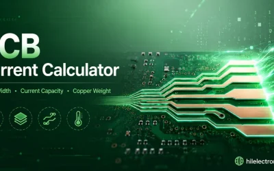
PCB Current Calculator: Sizing Trace Width and Vias with the IPC-2221 Formula
How a PCB current calculator works — the IPC-2221 trace width formula, internal vs external derating, copper weight, via current capacity, and a worked example you can follow step by step.
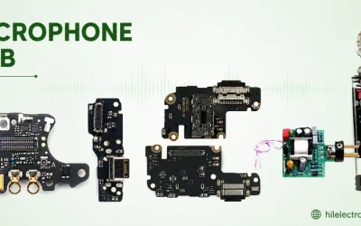
Microphone PCB Design: How the Board Itself Shapes Your Audio Quality
How a microphone PCB shapes audio quality — MEMS vs electret, top-port vs bottom-port sound holes, analog vs PDM/I2S output, grounding, and reflow. An assembly engineer’s design and sourcing guide.
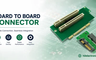
Board-to-Board Connector: Types, Specifications, and How to Select One
A deep guide to board-to-board connectors — mezzanine, right-angle, edge, and cable-to-board types; how pitch, stack height, current rating, mating cycles, and contact plating drive selection; plus signal-integrity, assembly, and rigid-flex alternatives.
Take a Quick Quote