
Back to blog
PCB Defects: Common type, Solutions, and Prevention

What are PCB Defects?
Common PCB defects refer to any anomalies or irregularities occurring during the manufacturing process that deviate from the intended design or function. These defects can arise at various stages of production, including etching, soldering, lamination, or even due to design flaws. The complex nature of PCBs, coupled with the miniaturization of electronic components, means that even the slightest deviation can lead to significant problems.
Defect prevention starts before fabrication, so common PCB defects should be tied back to design-for-manufacturing review and confirmed through suitable bare-board electrical testing.
The implications of PCB defects are far-reaching. In the best-case scenario, a defect might cause minor interference or reduced efficiency in a device. However, in more severe cases, these defects can lead to complete failure of the electronic device, risking data loss, operational downtime, and even physical danger if the device is a critical component in a safety system. In industries like aerospace, automotive, and healthcare, where reliability is paramount, the consequences of PCB defects can be particularly severe.
Diagnosing PCB Defects
Diagnosing defects in Printed Circuit Boards (PCBs) is a critical aspect of ensuring their functionality and reliability. Effective diagnosis not only helps in rectifying the current issues but also aids in enhancing the manufacturing process for future production. Here’s a detailed look at the techniques and tools used for identifying different types of PCB defects.
Techniques for Identifying PCB Defects
Visual Inspection: This is the most basic form of defect identification. Inspectors look for visible signs of defects such as cracks, misalignments, or soldering flaws. This method, while straightforward, might not detect microscopic or internal defects.
Automated Optical Inspection (AOI): This advanced technique uses high-resolution cameras to capture images of the PCB and compare them against a detailed schematic. AOI can detect a wide range of surface-level defects like scratches, stains, or incorrect component placement.
X-Ray Inspection: For internal defects that are not visible to the naked eye, X-ray inspection is used. This method can detect issues like layer misalignment, internal cracks, or voids in solder joints.
In-Circuit Testing (ICT): ICT involves testing the electrical performance of a PCB. It checks for shorts, opens, resistance, capacitance, and other electrical characteristics to ensure the board functions as intended.
Functional Testing: This involves testing the PCB in its final form, simulating the operational environment to ensure it performs its intended function.
Tools Used for Diagnosis
Magnifying Glasses and Microscopes: For manual visual inspections, various magnifying tools are used to identify surface defects.
AOI Machines: Equipped with sophisticated cameras and image processing software, these machines are essential for automated surface inspection.
X-Ray Machines: High-resolution X-ray machines provide detailed internal images of multi-layered PCBs, helping to identify hidden defects.
Multimeters and Oscilloscopes: Used in ICT, these tools measure the electrical properties of components and circuit paths.
Custom Testing Rigs: Developed for functional testing, these rigs are designed to test the PCB in conditions mimicking its final operational environment.
Types of Common PCB Defects and Solutions
1. Shorts and Opens
Definition: Shorts occur when unintended connections are made between circuit paths, while opens are breaks in the circuit that prevent current flow.
Causes: Shorts can be caused by excess solder bridging adjacent tracks, while opens are often due to incomplete soldering or damaged traces.
Solution: Use Automated Optical Inspection (AOI) to detect these issues. Improving solder paste application accuracy and enhancing the etching process can prevent such defects.
2. Solder Bridging
Description: Solder bridging happens when solder connects two or more adjacent pins that should not be connected, leading to a short circuit.
Impact: It can render a PCB non-functional by creating incorrect electrical pathways.
Solution: Reflow soldering techniques and careful stencil design can reduce solder bridging. AOI systems are also effective in detecting these issues early in the manufacturing process.
3. Annular Ring Issues
Explanation: Annular rings are the circular areas around drilled holes in a PCB. Issues arise when these rings are broken or incomplete.
Causes and Solutions: Proper alignment during drilling and ensuring adequate copper width around holes can prevent these issues. Inspection after drilling can catch and rectify any misalignments.
4. Acid Traps
Description: Acid traps occur when the PCB design leads to the accumulation of etching acids, causing over-etching in certain areas.
Problematic Nature: These can weaken the PCB and lead to circuit failures.
Solution: Designing wider angles in the PCB layout can prevent acid traps. Additionally, thorough cleaning post-etching helps remove any residual acids.
5. Delamination
Understanding: Delamination involves the separation of PCB layers, often due to high temperatures or moisture absorption.
Impact: It compromises the structural integrity and electrical functionality of the PCB.
Solution: Using high-quality materials and controlling the manufacturing environment (temperature and humidity) can significantly reduce the risk of delamination.
Prevention of PCB Defects
Preventing defects in Printed Circuit Boards (PCB) is essential for ensuring reliability and functionality in electronic devices. By adopting best practices in PCB design and manufacturing, many common defects can be avoided. Here are some key strategies for preventing PCB defects:
1. Adherence to Design Guidelines
Use of Standardized Layouts: Following industry-standard guidelines for PCB design helps in avoiding common pitfalls.
Design for Manufacturability (DFM): Incorporate DFM principles to ensure the PCB design is practical and feasible for manufacturing without defects.
Avoid Complex Designs When Unnecessary: Simplify the design where possible to minimize the chances of errors.
2. Quality Control in Manufacturing Process
Regular Inspection and Testing: Implementing regular inspection routines at each stage of the PCB manufacturing process helps in early detection of potential issues.
Automated Optical Inspection (AOI): Utilize AOI for detecting defects like shorts, opens, and solder bridging.
X-ray Inspection: For layered PCBs, X-ray inspection is effective in detecting internal defects which are not visible externally.
3. Material Quality and Handling
High-Quality Materials: Using high-grade materials reduces the chances of defects like delamination and warping.
Proper Storage and Handling: Ensure materials are stored and handled properly to prevent damage and contamination.
4. Environmental Control
Humidity and Temperature Control: Maintaining optimal environmental conditions during manufacturing prevents issues like delamination and misalignment.
Clean Manufacturing Environment: A clean and controlled environment prevents contamination that can lead to defects.
5. Skilled Workforce
Training and Expertise: Well-trained personnel are less likely to make errors in the manufacturing process.
Continuous Education: Keeping the workforce updated with the latest manufacturing techniques and standards.
6. Use of Advanced Manufacturing Techniques
Up-to-Date Equipment: Utilizing the latest manufacturing technologies can increase precision and reduce errors.
Process Optimization: Continually refining manufacturing processes to increase efficiency and reduce the likelihood of defects.
7. Collaboration with Suppliers
Choosing Reputable Suppliers: Working with reputable suppliers ensures that the materials and components used are of high quality.
Effective Communication: Clear communication about requirements and standards with suppliers can prevent misunderstandings that lead to defects.
Conclusion
Preventing PCB defects is a multifaceted approach that involves careful design, meticulous manufacturing processes, quality material selection, and skilled personnel. By implementing these prevention strategies, manufacturers can significantly reduce the incidence of defects, leading to more reliable and higher-quality PCBs. This not only saves costs in the long run but also ensures customer satisfaction and product reliability.
For production planning, it also helps to compare this topic with PCB quality assurance process and PCB conformal coating before finalizing the fabrication or assembly package.

Related Articles
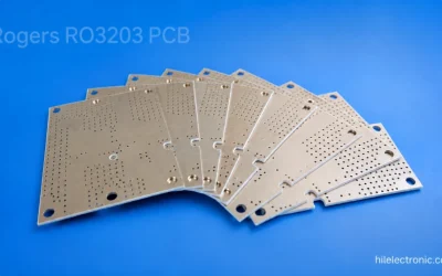
Rogers RO3203 PCB Manufacturing for Compact RF Circuits
Order custom RO3203 RF PCBs with controlled dielectric thickness, precision etching, impedance control, hybrid stackups and optional RF module assembly.
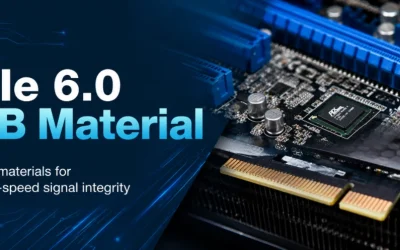
PCIe 6.0 PCB Material Selection for Motherboards, Risers and Add-In Cards
Manufacture PCIe 6.0 motherboards, risers and add-in cards with suitable low-loss materials, backdrilled vias, impedance control and optional PCB assembly.
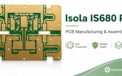
Isola IS680 PCB Manufacturer for Cost-Effective Low-Loss RF Boards
Evaluate IS680 as a practical PTFE alternative for commercial RF boards with exact grade control, low-loss fabrication and optional assembly.