
Back to blog
The meaning of Vias Plugged with Solder Mask oil on PCB

For the BGA pad shown in the picture, it is recommended that the via holes be filled with resin.
Introduction to Via Plugged and Its Importance in PCB Fabrication
Via Plugged is a process used in PCB fabrication to fill vias with a non-conductive material, such as solder mask or epoxy resin, to protect them from contamination and ensure their integrity. This technology has become increasingly important with the rise of high-density interconnect (HDI) PCB designs, where small vias are used to achieve greater routing density.
The primary purpose of via plugging is to prevent the ingress of contaminants, such as solder flux, chemicals, or moisture, which can lead to short circuits or other electrical failures. By filling the vias with a non-conductive material, the risk of contamination is greatly reduced, improving the overall reliability and longevity of the PCB.
There are several methods used for via Plugged, including solder mask plugging and epoxy resin plugging. Solder mask plugging involves filling the vias with solder mask material using a stencil printing process. This method is effective for small vias and provides good protection against contamination. Epoxy resin plugging, on the other hand, uses epoxy resin to fill the vias, providing excellent electrical insulation and mechanical strength.
Overall, via Plugged is a critical technology in PCB fabrication, essential for ensuring the reliability and performance of modern electronic devices. By understanding the importance of via plugging and using the right methods, PCB manufacturers can create high-quality boards that meet the demands of today’s electronic applications.
Understanding Via Plugged Technology
Via plugged is a critical step in PCB manufacturing, ensuring the reliability and performance of electronic devices. This process involves filling vias with a non-conductive material to prevent the infiltration of contaminants that could lead to short circuits or other failures. Here’s a detailed look at the importance of via plugging and the methods used in this process.
- Preventing Contamination: One of the primary purposes of via plugging is to prevent contamination. When vias are left open, flux, chemicals, or moisture can enter the holes during assembly or operation, leading to corrosion, electrical shorts, or other issues.
- Improving Electrical Performance: By filling vias with a non-conductive material, the electrical properties of the PCB can be enhanced. This is especially important for high-speed or high-frequency applications where signal integrity is critical.
- Enhancing Mechanical Strength: Filling vias with a solid material can also improve the mechanical strength of the PCB. This is particularly beneficial for boards that will be subjected to mechanical stress, such as those used in automotive or aerospace applications.
- Facilitating Assembly: Via plugging can also make the assembly process easier and more reliable. It can prevent solder paste from flowing through the vias during assembly, ensuring proper soldering and reducing the risk of defects.
- Types of Via Plugging:
- Solder Mask Plugging: In this method, vias are filled with solder mask material using a stencil printing process. This is a common method for small vias and offers good protection against contamination.
- Epoxy Resin Plugging: Epoxy resin is another common material used for via plugging. It provides excellent electrical insulation and mechanical strength, making it ideal for demanding applications.
- Considerations for Via Plugged :
- Size and Density of Vias: The size and density of vias on the PCB will influence the choice of plugging method. Smaller vias may require more precise and intricate plugging techniques.
- Material Compatibility: The plugging material should be compatible with the rest of the PCB materials to ensure proper adhesion and performance.
- Manufacturing Process: The chosen plugging method should be compatible with the overall PCB manufacturing process to ensure efficiency and reliability.
Overall, via plugged is a critical process in PCB manufacturing, offering several benefits in terms of reliability, performance, and ease of assembly. By understanding the importance of via plugging and choosing the right method for your PCB design, you can ensure the long-term functionality and durability of your electronic devices.
For a more complete production review, use this article alongside solder mask design review and BGA PCB assembly when checking stackup, assembly, or test requirements.
Key Characteristics of Via Plugging

Application Specificity: While the majority of vias on PCBs do not require exposure, certain vias, such as component plugging vias, thermal-dissipation vias, and test vias, necessitate specific treatment. Solder mask plugging effectively prevents flux or solder paste from seeping through vias during component assembly, thereby averting potential short circuits and conserving solder paste.
Compatibility with SMT Requirements: Solder mask-plugged vias address the stringent requirements of SMT by preventing adhesive or solder residues from migrating onto the surfaces of sensitive components, such as integrated circuits (ICs). This ensures clean and reliable soldering connections, essential for optimal PCB performance.
Protection Against Contamination: By sealing vias with solder mask, the ingress of flux, chemicals, or moisture into the narrow spaces between BGA components and PCBs is effectively mitigated. This reduces the risk of reliability issues stemming from contamination and facilitates easier cleaning processes during assembly.
Vacuum Compatibility: In automated assembly lines where vacuum transportation or inspection is employed, it is imperative to plug vias to prevent vacuum leakage. Unplugged vias can lead to instability in component fixation and pose challenges during manufacturing processes.
Causes of Poorly Executed Solder Mask Plugging
The efficacy of solder mask plugging hinges on the completeness and adequacy of the plugging process. Common causes of poorly executed plugging include:
- Incomplete or Insufficient Plugging: This occurs when there is an absence of solder mask oil at the top portion of vias, leaving only a minimal amount of solder mask at the bottom. Alternatively, air holes may develop along the via walls, leading to inadequate coverage and potential vulnerabilities.
- Solder Mask Defects: Defects in the solder mask, such as air bubbles or inconsistencies in application, can compromise the integrity of plugging and pave the way for contamination or etching of via copper during subsequent fabrication processes.
Consequences of Via Copper Damage
The ramifications of via copper damage resulting from poorly executed solder mask plugging can be far-reaching and detrimental to PCB performance:
- Increased Resistance: Thin or damaged via copper can significantly increase resistance, impairing electrical conductivity and leading to functional deficiencies in electronic devices. This may go undetected during initial testing, only manifesting as operational issues or failures during prolonged usage.
- Reliability Concerns: PCBs with compromised via copper are prone to reliability issues, including intermittent connectivity, signal degradation, and premature component failure. These issues can undermine the overall reliability and lifespan of electronic products, leading to costly recalls or warranty claims.
- Manufacturing Challenges: Identifying and rectifying via copper damage post-fabrication can pose significant challenges for PCB manufacturers, potentially resulting in scrapped batches and production delays. Moreover, the detection of via copper damage may necessitate advanced testing techniques beyond conventional inspection methods.
Effective Solutions and Recommendations
Addressing the challenges posed by poorly executed solder mask-plugged vias requires a multifaceted approach encompassing design optimization, process refinement, and quality assurance measures:
- Engineering Design Considerations: PCB designers should pay close attention to via plugging aperture and fullness specifications, ensuring that design files adhere to industry standards and manufacturing capabilities. Optimal via plugging fullness, typically exceeding 75%, should be stipulated to mitigate the risk of incomplete plugging.
- Technological Advancements: PCB manufacturers should explore advanced solder mask plugging technologies that offer high plugging fullness and reliability. Technologies such as resin plugging and surface finish integration hold promise for enhancing plugging efficacy while streamlining manufacturing processes.
- Rigorous Quality Control: Comprehensive testing and validation of solder mask materials and plugging processes are essential to ensure compliance with quality standards and specifications. Technological tests should be conducted on new solder mask oils and resins to assess their performance and reliability in real-world applications.
- Enhanced Inspection Protocols: Electrical testing should be leveraged to detect anomalies such as thin via copper or circular breakage indicative of solder mask plugging defects. Close collaboration between engineering and quality assurance teams can facilitate the early identification and resolution of plugging-related issues.
Conclusion
Overall, via plugging is a critical technology in PCB fabrication, essential for ensuring the reliability and performance of modern electronic devices. By preventing the ingress of contaminants and providing mechanical strength to vias, plugging contributes to the longevity of PCBs. However, poorly executed plugging can lead to severe consequences, including increased resistance, reliability issues, and manufacturing challenges.
To address these challenges, PCB designers and manufacturers must prioritize engineering design considerations, adopt advanced plugging technologies, and implement rigorous quality control measures. By doing so, they can mitigate the risks associated with poorly executed plugging and ensure the long-term functionality and durability of electronic devices.
PCB & PCBA Quick Quote
Related Articles
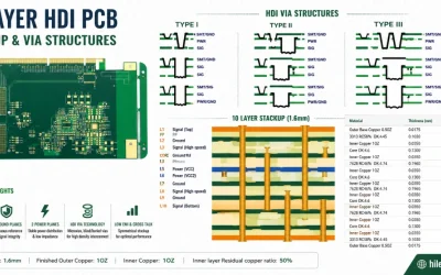
10 Layer HDI PCB Engineering for Microvias and BGA Escape
10 layer HDI PCB engineering guidance for 1+8+1, 2+6+2 and 3+4+3 buildups, microvia reliability, BGA escape, materials and inspection.
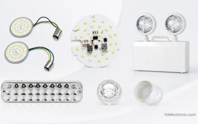
LED Emergency & Exit Light PCBs: Battery-Backed Boards, Self-Test & Driver Electronics
Manufacture LED emergency light PCBs for battery backup, charging, self-test logic, transfer circuits, drivers and exit-sign assemblies.
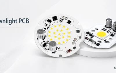
LED Downlight PCBs: Round Light Engines, Drivers & Dimming Boards for Recessed Fixtures
Get LED downlight PCB fabrication and assembly for round light engines, compact drivers, TRIAC, 0-10 V and DALI dimming boards.