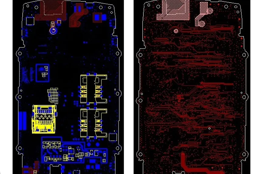
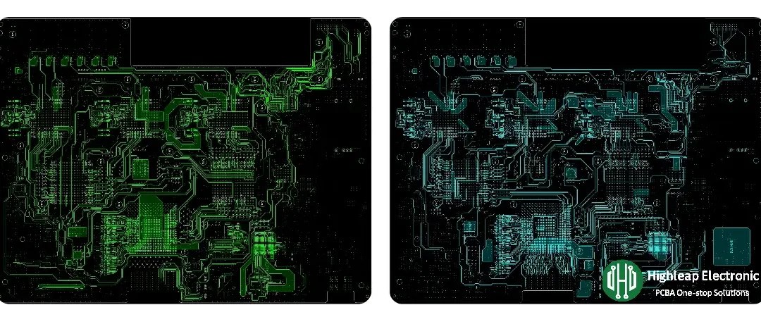
Select Page

Your PCB Manufacturing Expert – Highleap Electronic

The True Blind Buried Via PCB Cost Breakdown

The True Blind Buried Via PCB Cost Breakdown

Table of Contents Blind Buried Via PCB Cost: What the Per-Board Price Actually Covers Material Grade Impact on Blind Buried Via PCB Cost Manufacturing Process Cost: Lamination, Drilling, and Plating Testing and Quality Assurance Costs NRE and Tooling: One-Time Costs...

HDI Blind Via PCB Cost Drivers Lamination Drill and Design

HDI Blind Via PCB Cost Drivers Lamination Drill and Design

Table of Contents HDI Blind Via PCB Cost Drivers 1+N+1 vs. 2+N+2 vs. Any-Layer: Cost Progression Laser vs. Mechanical Drilling Economics Via Filling and Stacking Cost Impact Design Decisions That Control Cost Volume Economics and NRE Amortization Cost-Optimized HDI...

Blind Via PCB Price Per Board and HDI Cost Analysis

Blind Via PCB Price Per Board and HDI Cost Analysis

Table of Contents What Determines Blind Via PCB Price: The Cost Structure Breakdown Laser Drilling vs. Mechanical Drilling: Cost Structure and Selection Logic How Via Count, Geometry, and Fill Specification Drive Price Volume Pricing, NRE Amortization, and Repeat...

Mobile PCB Fabrication and Assembly

Mobile PCB Fabrication and Assembly

Smartphone PCBs are among the most demanding circuit boards manufactured at scale—10 to 12 copper layers compressed into under 1mm of thickness, carrying signals from DC power rails to 40GHz 5G antenna feeds simultaneously. Manufacturing them reliably requires a...

Phone Circuit Board Manufacturing and HDI Assembly

Phone Circuit Board Manufacturing and HDI Assembly

Every smartphone depends on a phone circuit board engineered to tolerances measured in microns—a multi-layer laminated assembly where copper pathways thinner than a human hair carry signals between hundreds of components at frequencies from DC power to millimeter-wave...

Blind and Buried Via PCB Quote Guide for HDI Boards

Blind and Buried Via PCB Quote Guide for HDI Boards

Our Blind and Buried Via PCB technology offers advanced manufacturing for high-layer, high-speed boards, ideal for industries like telecommunications, aerospace, and high-performance computing. Understand the key factors that influence cost and lead time in our...

HDI Stackup Design Guide for Production-Ready PCBs

HDI Stackup Design Guide for Production-Ready PCBs

A production-ready HDI stackup is not a “layer count decision.” It is a controlled construction plan that defines how build-up layers, microvias, dielectric thickness, copper build, and reference planes work together to achieve routing density without sacrificing...