Select Page

Your PCB Manufacturing Expert – Highleap Electronic

Essential PCB Power Integrity Design Guide

Essential PCB Power Integrity Design Guide

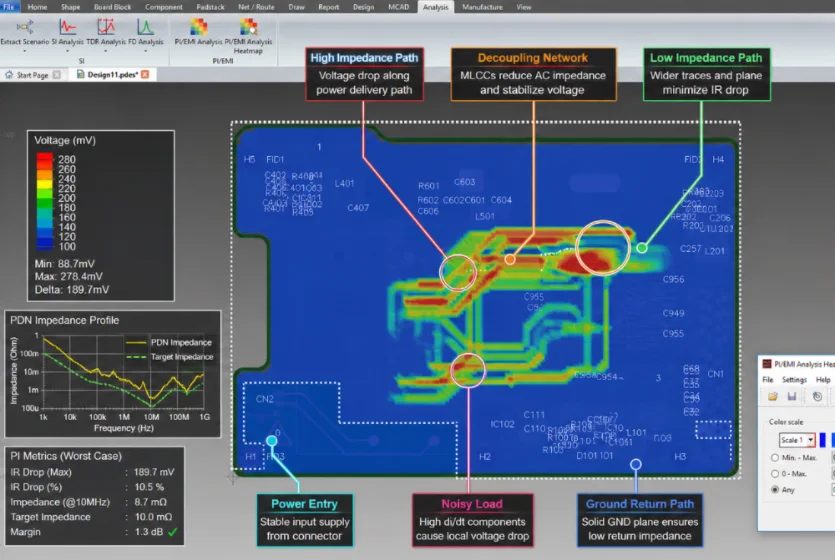
Table of Contents What Is PCB Power Integrity and Why It Matters PDN Fundamentals and Target Impedance Power Plane and Ground Plane Design Decoupling Capacitor Strategy Simultaneous Switching Noise (SSN) Control PI vs SI: Key Interactions PI Design Checklist Before...

Schematic Meaning for PCB Design and Manufacturing

Schematic Meaning for PCB Design and Manufacturing

In electronics, schematic meaning refers to the logical representation of a circuit using standardized symbols and electrical connections. A schematic shows how components are connected, how signals flow, and how the circuit is intended to work before PCB design and...

HDI Stackup Design Guide for Production-Ready PCBs

HDI Stackup Design Guide for Production-Ready PCBs

A production-ready HDI stackup is not a “layer count decision.” It is a controlled construction plan that defines how build-up layers, microvias, dielectric thickness, copper build, and reference planes work together to achieve routing density without sacrificing...

Copper Pour and Via Stitching: A Technical Guide for PCB Design

Copper Pour and Via Stitching: A Technical Guide for PCB Design

Introduction: Understanding Copper Pour and Via Stitching Copper pour refers to filling large areas of a PCB layer with copper to serve specific electrical or thermal functions. Via stitching involves placing multiple vias to connect copper regions across different...

PCB Shape: A Comprehensive Guide to Board Geometry Selection

PCB Shape: A Comprehensive Guide to Board Geometry Selection

1. Introduction: PCB Shape Definition and Strategic Importance PCB shape refers to the physical outline or geometric form of a printed circuit board. This fundamental design parameter extends beyond aesthetics—it directly influences component placement efficiency,...

Fiducial Marks on PCB: Complete Design & Placement Guide

Fiducial Marks on PCB: Complete Design & Placement Guide

[pac_divi_table_of_contents title="On this article" default_state="closed" included_headings="off|on|off|off|off|off" exclude_headings_by_class="on" active_link_highlight="on" level_markers_3="icons" title_container_padding="10px|15px|10px|15px|true|false"...

What Is GND in Electronics? Understanding the Ground Reference

What Is GND in Electronics? Understanding the Ground Reference

[pac_divi_table_of_contents title="On this article" default_state="closed" included_headings="off|on|off|off|off|off" exclude_headings_by_class="on" active_link_highlight="on" level_markers_3="icons" title_container_padding="10px|15px|10px|15px|true|false"...

RF Simulation Tools for PCB Design: A Comprehensive Guide

RF Simulation Tools for PCB Design: A Comprehensive Guide

[pac_divi_table_of_contents title="On this article" default_state="closed" included_headings="off|on|off|off|off|off" exclude_headings_by_class="on" active_link_highlight="on" level_markers_3="icons" title_container_padding="10px|15px|10px|15px|true|false"...