
Heavy Copper PCB Design for Power Electronics: A Practical Engineering Guide

Power electronics demand PCB solutions capable of handling high currents while maintaining thermal stability and long-term reliability. Heavy copper PCB design addresses these challenges through increased copper thickness, specialized layout strategies, and enhanced thermal management techniques.
This guide examines the critical design considerations for heavy copper PCB applications, from initial layout decisions to manufacturing feasibility, focusing on practical implementation in DC-DC converters, motor drives, inverters, and industrial power supplies.
What Is a Heavy Copper PCB and Why It Matters in Power Electronics
Defining Heavy Copper Construction
Heavy copper PCBs feature copper weights of 3 oz/ft² or greater, compared to standard PCBs that typically use 1 oz/ft² copper. This increased copper thickness directly enhances current carrying capacity, reduces resistive losses, and improves heat dissipation across the board.
Performance Advantages in Heavy Copper PCB Design
The primary benefits of heavy copper construction include:
- Higher current capacity – Thicker copper reduces electrical resistance, enabling 20-50A continuous currents per trace without excessive heating
- Superior heat dissipation – Enhanced thermal conductivity spreads heat across larger areas, reducing hot spots and thermal stress
- Improved mechanical strength – Increased copper mass provides better resistance to thermal cycling and mechanical stress
- Lower voltage drop – Reduced trace resistance minimizes power losses in high-current pathways
Application Areas
Heavy copper PCB design serves automotive inverters, onboard chargers, industrial motor controllers, and high-power LED drivers. These applications require continuous high-current operation, efficient heat removal, and reliable performance under sustained electrical and thermal stress.
Heavy Copper PCB Design: Layout Guidelines
Minimizing Power Loop Impedance
Effective layout optimization focuses on reducing the power loop area. Place input capacitors close to switching devices and maintain short, direct current paths to minimize parasitic inductance. This reduces voltage overshoot, electromagnetic interference, and switching losses.
Current Path Distribution Strategy
Distribute high-current traces across multiple layers when possible, avoiding bottleneck regions where current must funnel through narrow sections. Wide copper pours and filled planes provide low-impedance power distribution while naturally spreading heat across larger board areas.
Creepage and Clearance Requirements
Heavy copper PCB design must account for increased spacing requirements due to higher voltages. Maintain adequate creepage distances between high-voltage nodes according to applicable safety standards. Thicker copper requires larger clearances during etching to prevent shorts between adjacent traces.
Copper Thickness Selection and Trace Width Calculation
Determining Required Copper Weight
Select copper thickness based on maximum continuous current and acceptable temperature rise. Common heavy copper weights range from 2 oz/ft² for moderate power applications to 10 oz/ft² for extreme current densities. Each doubling of copper thickness approximately doubles the current capacity for a given trace width.
IPC-2152 Standards and Calculations
The IPC-2152 standard provides empirical data for trace width calculations in heavy copper PCB design, accounting for copper weight, ambient temperature, and allowable temperature rise. For a 3 oz copper trace carrying 20A with 30°C rise, expect widths around 5-8mm depending on whether the trace is internal or external.
Manufacturing Tolerance Considerations
Increased copper thickness affects etching precision, typically resulting in greater line width variation. Design rules should account for over-etch effects that become more pronounced with thicker copper. Work with minimum trace widths of 8-10 mils for 3-4 oz copper, scaling upward for heavier weights.

Heavy Copper PCB
Via Design for High Current and Thermal Conduction
Current Transfer Via Arrays
Heavy copper PCB design requires robust via structures to transfer current between layers without creating bottlenecks. Single vias prove inadequate for high currents; instead, use arrays of multiple parallel vias. For a 20A path, distribute 10-15 vias across the connection area to ensure adequate current capacity and thermal performance.
Thermal Via Implementation
Thermal vias beneath power components provide critical heat conduction paths from hot surfaces to internal copper planes and bottom-side heatsinks. Arrange thermal vias in dense arrays with typical spacing of 20-30 mils. Filled and plated vias offer superior thermal performance compared to unfilled vias.
Via Plating Quality Standards
Maintain minimum via diameters of 0.3mm (12 mils) to ensure reliable copper plating coverage throughout the hole depth. Heavy copper boards require thicker plating to achieve adequate copper distribution through the via barrel, particularly for aspect ratios exceeding 8:1.
Thermal Management in Heavy Copper PCB Design
Copper Plane Heat Spreading
Heavy copper construction inherently provides excellent lateral heat spreading through thick internal planes. Use 2-4 oz copper for internal power and ground planes to create effective thermal distribution layers that conduct heat away from hot spots and distribute it across the board area.
Metal Core Integration
For extreme thermal demands, combine heavy copper PCB design with metal core substrates. Aluminum or copper cores provide direct thermal paths from component mounting areas to external heatsinks. This approach proves particularly effective for high-density power converters and LED applications.
Strategic Thermal Via Placement
Position thermal via arrays strategically beneath MOSFETs, diodes, and other heat-generating components. A typical power MOSFET may require 30-50 thermal vias within its thermal pad footprint to adequately conduct heat away from the junction.
Manufacturing Considerations for Heavy Copper PCB Design
Etching Process Limitations
Thicker copper requires longer etch times, increasing the risk of over-etch and trace undercutting. Expect minimum feature sizes to scale with copper weight:
- 2-3 oz copper – Minimum trace and space of 6-8 mils
- 4 oz copper – Minimum trace and space of 10-12 mils
- 6 oz copper – Minimum trace and space of 15-18 mils
- 8-10 oz copper – Minimum trace and space of 20+ mils
Plating and Via Filling
Via plating becomes progressively more difficult as copper weight increases, particularly for high aspect ratio holes. Filled vias in heavy copper boards require specialized plating processes and multiple plating cycles. Communicate stack-up and via requirements with manufacturers early in the design phase.
Layer Stack-Up Design
Heavy copper layers create challenges in layer-to-layer registration and lamination uniformity due to significant thickness variations. Design symmetric stack-ups when possible to balance mechanical stresses and prevent board warpage during fabrication or assembly.
Design Optimization Tips
Simulation and Verification
Validate heavy copper PCB design using thermal simulation tools before manufacturing. Software such as Ansys SIwave, Altium PDN Analyzer, or thermal FEA tools predict current distribution, temperature profiles, and potential hot spots. These simulations inform trace width adjustments and thermal management improvements.
Design Rule Balancing
Optimize by balancing electrical performance requirements against manufacturing constraints. While 6 oz copper provides excellent current capacity, 3-4 oz copper often suffices while offering better etching precision and lower cost. Analyze actual operating currents and duty cycles to avoid over-specification.
Manufacturer Collaboration
Engage PCB manufacturers during the design phase to understand their specific heavy copper capabilities, design rules, and cost drivers. Request design for manufacturing feedback on copper distribution, via patterns, and minimum features to prevent costly redesigns.
Conclusion
Heavy copper PCB design requires systematic attention to current capacity, thermal management, and manufacturing feasibility. Success depends on understanding the relationship between copper thickness, trace geometry, via construction, and heat dissipation pathways. Engineers who master these interconnected factors create power electronics that deliver reliable performance under demanding conditions.
At Highleap Electronics, we provide comprehensive heavy copper PCB manufacturing capabilities:
- Custom copper thickness – 2 oz to 10 oz copper weight options tailored to your current requirements
- Advanced via technology – Filled, plated, and thermal via arrays for optimal electrical and thermal performance
- Thermal management support – Metal core integration and strategic copper plane design for efficient heat dissipation
- Design collaboration – Engineering review and DFM feedback to ensure first-pass manufacturing success
Contact our engineering team to discuss your power electronics requirements and learn how our heavy copper PCB design and manufacturing expertise can support your next project.

Recommended Posts
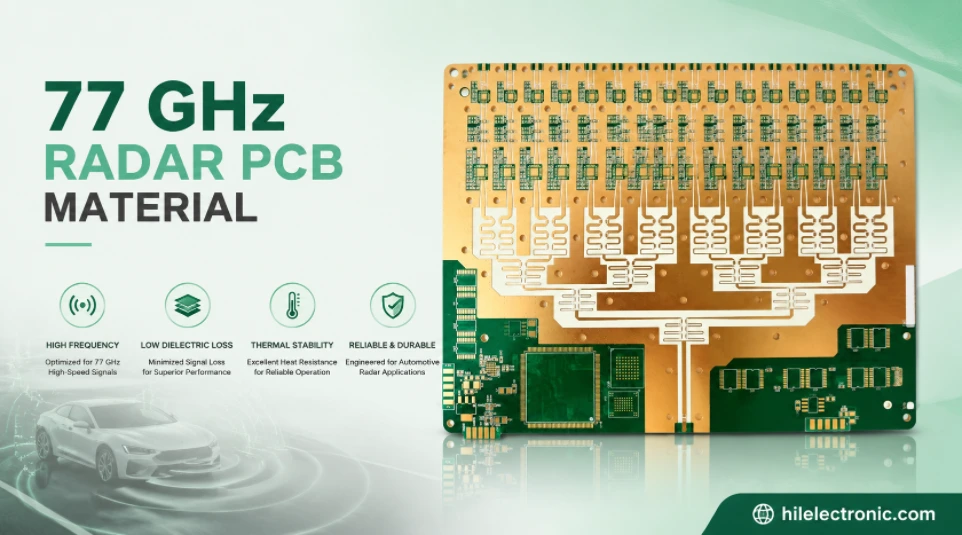
77 GHz Radar PCB Material Selection and Manufacturing Guide
Table of contentsWhat 77 GHz Changes in a PCBCommon 77 GHz...
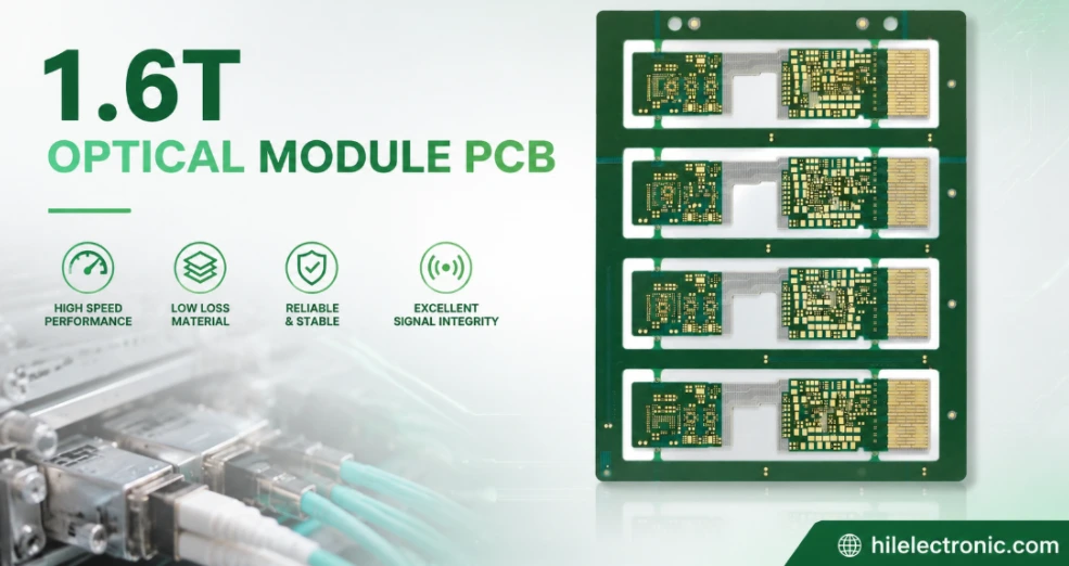
1.6T Optical Module PCB Manufacturing and Assembly Service
Table of contents1.6T Module Architectures and PCB...
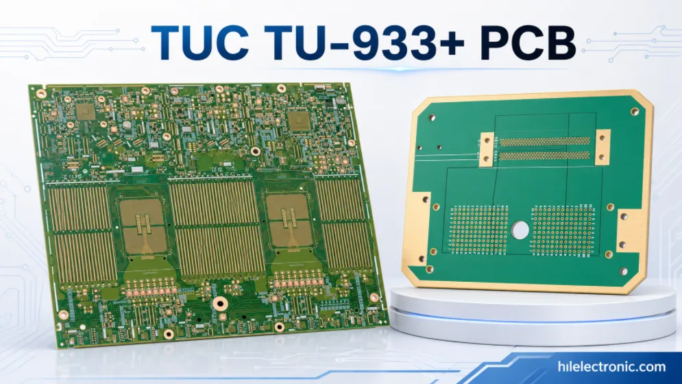
TUC TU-933+ PCB Manufacturing for Super-Low-Loss High-Speed Systems
Table of contentsWhat Is TU-933+ PCB Material?Why TU-933+...
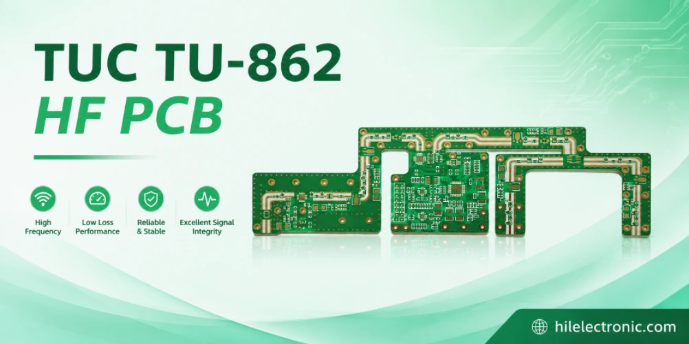
TUC TU-862 HF PCB Manufacturing and Assembly Service
Table of contentsWhat Is TU-862 HF?Why Choose TU-862 HF...
How to get a quote for PCBs
Let‘s run DFM/DFA analysis for you and get back to you with a report. You can upload your files securely through our website. We require the following information in order to give you a quote:
-
- Gerber, ODB++, or .pcb, spec.
- BOM list if you require assembly
- Quantity
- Turn time
In addition to PCB manufacturing, we offer a comprehensive range of electronic services, including PCB design, PCBA, and turnkey solutions. Whether you need help with prototyping, design verification, component sourcing, or mass production, we provide end-to-end support to ensure your project’s success.
For PCBA services, please provide your BOM (Bill of Materials) and any specific assembly instructions. We also offer DFM/DFA analysis to optimize your designs for manufacturability and assembly, ensuring a smooth production process.