
Comprehensive Guide to Heavy Copper PCBs

What is Heavy Copper PCB?
Heavy copper PCBs, also known as heavy copper weight PCBs, are circuit boards with copper thicknesses exceeding the typical range found in standard PCBs. While standard PCBs usually have copper thicknesses ranging from 1 oz to 3 oz (35 μm to 105 μm), heavy copper PCBs have copper thicknesses greater than 2 oz (70 μm). The term “heavy copper” is preferred over “thick copper” to describe these PCBs.
The copper weight of heavy copper PCBs can vary, with common weights including 2 oz (70 μm), 3 oz (105 μm), 4 oz (140 μm), 6 oz (210 μm), 8 oz (280 μm), and 10 oz (350 μm). The increased copper thickness in heavy copper PCBs provides several advantages, such as improved thermal performance and enhanced current carrying capacity.
Heavy copper PCBs are typically compatible with FR-4 dielectric material, which is commonly used in PCB manufacturing. Plated through holes (PTHs) in heavy copper PCBs often require filling or plugging to ensure proper electrical connections.
Manufacturing heavy copper PCBs requires careful attention to registration and lamination processes to ensure the copper layers are properly aligned and bonded to the PCB substrate. The use of heavy copper inner layers in these PCBs significantly improves their thermal performance and current carrying capacity, making them particularly suitable for applications such as LED lighting, power electronics, and electric vehicle inverters.
Advantages of Heavy Copper PCBs
Heavy Copper PCBs (Printed Circuit Boards) offer several advantages that make them suitable for specific applications, especially those that require high power or enhanced thermal management. Here are the advantages of Heavy Copper PCBs:
1. Excellent High Heat Resistance
Heavy copper PCBs have superior heat resistance due to their thick copper layers, allowing them to handle high temperatures without degradation. This makes them suitable for applications with demanding thermal requirements.
2. Excellent Current Carrying Capacity
Heavy copper PCBs can carry larger currents with the same line width compared to standard PCBs. The increased copper thickness reduces resistance, minimizing voltage drops and allowing for efficient current flow.
3. Reduced Complex Wiring Configuration
The increased copper thickness in heavy copper PCBs enables the consolidation of complex wiring configurations into a single layer. This simplifies the PCB design, reduces the number of layers required, and improves overall efficiency.
4. Compression of Board Size
Heavy copper PCBs allow for the compression of board size by combining multiple copper weights on the same PCB. This space-saving feature is especially beneficial in applications with size constraints.
5. Incorporation of Different Copper Weights
Heavy copper PCBs can incorporate different copper weights on the same circuit layer. This allows for the integration of high-power and low-power circuits, providing flexibility in designing diverse functionality within a single PCB.
6. Support for High-Temperature Materials
Heavy copper PCBs can support the use of special high-temperature materials, reducing the risk of circuit failure under extreme temperature conditions. This makes them suitable for applications that operate in high-temperature environments.
7. Enhanced Mechanical Strength
The thick copper layers in heavy copper PCBs enhance the mechanical strength of the PCB, particularly in the connector area, plated through-holes (PTH), and pads. This improves the overall durability and reliability of the PCB.
8. Integrated High-Current Circuits and Impedance Control
Heavy copper PCBs allow for the integration of high-current circuits and impedance control on a single PCB. This simplifies the design and manufacturing process, reducing complexity and improving overall performance.
9. Built-in Cooling
Partially plating heavy copper on specific areas of the PCB can provide built-in cooling capabilities. The thick copper layers help dissipate heat from components, improving thermal management and reducing the need for additional cooling mechanisms.
10. Size Reduction of End-Use Products
The use of heavy copper PCBs can help reduce the size of end-use products. The enhanced current carrying capacity and heat dissipation capabilities allow for more compact designs without compromising performance.
These advantages make heavy copper PCBs a preferred choice for applications that require high power, high currents, thermal management, and compact designs. However, it’s important to consider the specific requirements of each application and consult with experienced PCB manufacturers to ensure the optimal use of heavy copper PCBs.
Ordinary PCB VS Heavy Copper PCB
When comparing ordinary PCBs (standard PCBs) to heavy copper PCBs, several key differences and considerations come into play. Here’s a comparison between the two:
Copper Thickness
- Ordinary PCBs: Standard PCBs typically have thinner copper layers, typically ranging from 1 to 2 ounces (35 to 70 μm) of copper thickness.
- Heavy Copper PCBs: Heavy copper PCBs, as the name suggests, have significantly thicker copper layers. The copper thickness in heavy copper PCBs ranges from 3 ounces (105 μm) and can go up to 20 ounces (700 μm) or more.
Current Carrying Capacity
- Ordinary PCBs: Standard PCBs have limited current carrying capacity due to their thinner copper layers. They are suitable for low to moderate current applications.
- Heavy Copper PCBs: Heavy copper PCBs excel in high-current applications. The increased copper thickness allows them to handle larger currents without excessive heating or voltage drops. They can efficiently carry high currents without compromising performance.
Thermal Management
- Ordinary PCBs: Standard PCBs usually have limited thermal management capabilities due to their thinner copper layers. Heat dissipation can be challenging, especially in high-power applications.
- Heavy Copper PCBs: Heavy copper PCBs offer excellent thermal management due to their thicker copper layers. The increased copper mass acts as an effective heat sink, distributing and dissipating heat more efficiently. This makes them ideal for applications that generate significant heat or require efficient heat dissipation.
Mechanical Strength
- Ordinary PCBs: Standard PCBs have moderate mechanical strength. They are generally suitable for typical applications and can withstand normal handling and environmental conditions.
- Heavy Copper PCBs: Heavy copper PCBs have enhanced mechanical strength due to their thicker copper layers. They exhibit better resistance to bending, warping, and mechanical stress. This makes them more durable and robust, suitable for applications that require higher mechanical reliability.
Cost and Complexity
- Ordinary PCBs: Standard PCBs are generally less expensive compared to heavy copper PCBs. They are also easier to manufacture and require less specialized equipment and processes.
- Heavy Copper PCBs: Heavy copper PCBs tend to be more expensive due to the higher cost of materials and the specialized manufacturing processes involved. They require additional steps and expertise to handle the thicker copper layers.
Design Flexibility
- Ordinary PCBs: Standard PCBs offer flexibility in terms of trace routing and density. They are suitable for general-purpose applications with average design requirements.
- Heavy Copper PCBs: Heavy copper PCBs offer increased design flexibility due to their ability to handle high currents and dissipate heat efficiently. Designers can use wider traces, larger vias, and increased copper pour areas without compromising performance, allowing for more intricate and specialized designs.
It’s important to note that the choice between ordinary PCBs and heavy copper PCBs depends on the specific requirements of the application. Standard PCBs are suitable for many everyday electronic devices, while heavy copper PCBs are favored in high-power applications that demand higher current carrying capacity, better thermal management, and increased mechanical strength.
Characteristics of Heavy Copper PCB
Heavy copper PCBs offer distinct advantages in electronics, such as handling higher currents, enhancing thermal management, and providing exceptional mechanical strength. Additional characteristics include:
- High Mechanical Strength: Superior resistance to bending, warping, and stress, ensuring durability and reliability.
- Excellent Weather Resistance: Suitable for outdoor or harsh conditions, withstanding temperature variations, moisture, and UV exposure without performance compromise.
- Superior Thermal Management: Effectively dissipates heat generated by power components, reducing overheating risks and enhancing overall performance.
- Effective Current Conduction: Reduced resistance and ample copper cross-sectional area improve current flow, minimizing voltage drops and ensuring reliable power delivery.
- Versatility in Design and Application: Suitable for power electronics, automotive systems, renewable energy, and industrial equipment due to their high current handling, heat dissipation, and mechanical strength.
- Enhanced Extendability and Performance: Enables integration of high-power components and advanced functionality within a single board, extending PCB capabilities and performance.
Heavy copper PCBs require specialized manufacturing processes and expertise. Collaborating with experienced PCB manufacturers ensures proper fabrication and optimal performance.
Heavy Copper PCB Design Guidelines
Designing heavy copper PCBs requires careful consideration of various factors to ensure optimal performance and manufacturability. Here are some key design guidelines to follow:
Layer Stacking
- Position thick copper layers close to the center of the PCB to minimize warpage issues.
- Avoid placing outer layers adjacent to each other, as this can exacerbate registration problems.
- Rotate the fiber weave direction by 90° between adjacent dielectric layers to enhance the board’s stability.
Component Placement
- Ensure sufficient clearance between components and plane layers to allow for proper soldermask coverage.
- Account for component shadows falling on inner copper layers to avoid potential short circuits.
- Check for any exposed copper at drilled holes, as it can lead to electrical connectivity issues.
Thermal Management
- Place heat-generating components directly over thick copper layers to utilize them as heat spreaders.
- Provide multiple vias beneath hot components to facilitate heat transfer to inner copper planes for efficient thermal management.
High Current Traces
- Utilize copper pouring or polygons for high current lines instead of routing multiple parallel traces. This minimizes resistance and improves current carrying capacity.
- Place high current traces adjacent to plated through-hole (PTH) vias to enhance heat dissipation.
Filled Vias
- Limit the use of filled vias, as they can impair heat transfer compared to hollow vias.
- If filled vias are necessary, countersink them and ensure that the soldermask is clear of the holes to avoid any manufacturing or assembly issues.
Panel and Tooling
- Allow generous tolerances in the design to account for material shrinkage, stretching, and warpage during fabrication and assembly processes.
- Incorporate fiducials and test coupons on the panel to facilitate easy tooling and alignment during manufacturing.
DFM Analysis
- Seek Design for Manufacturability (DFM) feedback from the PCB fabricator during the design phase.
- Check the manufacturability of the design, particularly regarding tolerance issues related to heavy copper.
- Engage with the PCB manufacturer early in the design process to address any potential issues and ensure a smooth prototyping and production phase.
By following these design guidelines and collaborating closely with the PCB manufacturer, you can optimize the design of heavy copper PCBs for superior performance, reliability, and manufacturability.
Applications of Heavy Copper PCB
Heavy copper PCBs have a wide range of applications across different industries. Some of the specific applications where heavy copper PCBs are commonly used include:
Computers: Heavy copper PCBs are utilized in high-performance computer systems, servers, and data centers where efficient power distribution and thermal management are crucial.
Solar Engineering: Heavy copper PCBs are employed in solar panels and solar power systems to handle high currents and ensure reliable power transmission.
Automobiles: Heavy copper PCBs are used in automotive electronics, such as engine control units (ECUs), powertrain systems, and electric vehicle charging infrastructure, where they provide robust power handling capabilities and thermal management.
Railways: Heavy copper PCBs are utilized in railway systems for signaling, power distribution, and control applications, where they can handle high currents and withstand harsh environmental conditions.
Military and Aerospace: Heavy copper PCBs are employed in military and aerospace applications that demand high reliability, durability, and resistance to extreme temperatures and vibrations.
Nuclear Power: Heavy copper PCBs are used in nuclear power plants for control systems, instrumentation, and power distribution, where they can handle high currents and ensure reliable operation under challenging conditions.
Medical: Heavy copper PCBs find application in medical devices and equipment, such as imaging systems, patient monitoring devices, and diagnostic equipment, where they provide robust power delivery and thermal management.
Industrial Control: Heavy copper PCBs are used in industrial control systems, motor drives, and power electronics applications that require efficient power handling and thermal dissipation.
LED Lighting: Heavy copper PCBs are employed in high-power LED lighting applications, where they can efficiently transmit power and dissipate heat, ensuring optimal performance and longevity of the LED lights.
Power Supplies: Heavy copper PCBs are utilized in power supply units (PSUs) and converters where high current carrying capacity and efficient heat dissipation are critical.
These are just a few examples of the diverse applications of heavy copper PCBs. Their unique characteristics, such as high current handling, thermal management capabilities, and mechanical strength, make them suitable for various industries and demanding applications.
Conclusion
Overall, heavy copper PCBs offer a reliable solution for high-power applications, and partnering with a reputable PCB manufacturer like Highleap can ensure the best results. With their expertise in PCB and PCBA manufacturing, Highleap can provide guidance and support throughout the design and fabrication process. By leveraging the advantages of heavy copper PCBs and collaborating with Highleap, industries can confidently meet the demands of high-power applications with superior quality and reliability.
FAQs
How do heavy copper PCBs improve thermal management?
Heavy copper PCBs improve thermal management through their thick copper layers, which act as effective heat sinks, dissipating heat more efficiently and reducing the risk of overheating.
Can heavy copper PCBs handle high-current applications?
Yes, heavy copper PCBs are designed to handle high-current applications. Their thick copper layers provide excellent current carrying capacity, minimizing voltage drops and ensuring efficient power delivery.
What are the cost implications of using heavy copper PCBs?
Heavy copper PCBs tend to be more expensive due to the higher cost of materials and specialized manufacturing processes. However, they offer significant benefits in terms of performance, reliability, and durability, making them a worthwhile investment for high-power applications.
What industries benefit most from heavy copper PCBs?
Industries such as automotive, aerospace, military, renewable energy, and industrial control benefit the most from heavy copper PCBs due to their high current handling, thermal management capabilities, and mechanical strength.
What design considerations are crucial for heavy copper PCBs?
Key design considerations for heavy copper PCBs include proper layer stacking to minimize warpage, strategic component placement for thermal management, and ensuring adequate clearances for soldermask coverage and electrical connectivity.

Recommended Posts
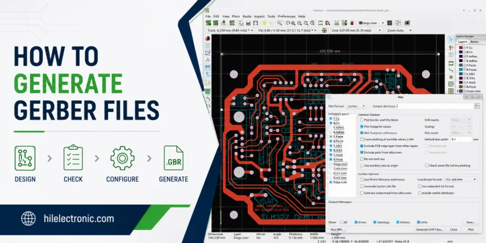
How to Generate Gerber Files for PCB Manufacturing
Figure 1. how to generate Gerber files image for Highleap...
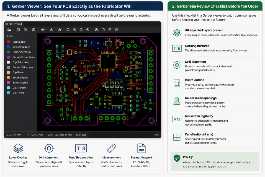
Gerber File Review Checklist: How to Check PCB Files Before You Order
Figure 1. Gerber file review catches missing layers, drill...
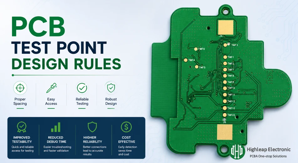
PCB Test Point Design Rules for Debug and ICT
Figure 1. PCB test point design rules help make debugging,...

PCB Jumper Wire: Uses, Types, and Design Tips
Figure 1. PCB jumper wires are useful for prototypes and...
Discover how our expertise can help with your next PCB project.