Select Page

Your PCB Manufacturing Expert – Highleap Electronic

Professional AI Motherboard PCB Manufacturing Solutions

Professional AI Motherboard PCB Manufacturing Solutions

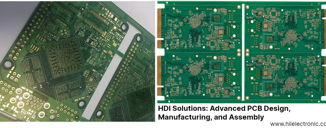
AI Motherboard Architecture and Technical Requirements AI motherboard PCB manufacturing demands premium materials and specialized processes to achieve the performance and reliability required for mission-critical AI applications. AI motherboard PCBs differ...

HDI PCB Guidelines for Server Motherboards

HDI PCB Guidelines for Server Motherboards

[pac_divi_table_of_contents title="On this article" default_state="closed" included_headings="off|on|off|off|off|off" exclude_headings_by_class="on" active_link_highlight="on" level_markers_3="icons" title_container_padding="10px|15px|10px|15px|true|false"...

HDI PCB Manufacturing Services in China | Cost-Optimized

HDI PCB Manufacturing Services in China | Cost-Optimized

In the realm of high-performance electronics, High-Density Interconnect (HDI) PCBs are indispensable for enabling compact, efficient, and reliable designs. At Highleap Electronic, a trusted HDI PCB manufacturer, we specialize in HDI PCB Manufacturing and Assembly,...

Expert High Density PCB Solutions by Highleap Electronic

Expert High Density PCB Solutions by Highleap Electronic

In the dynamic world of electronics, the demand for smaller, more powerful, and highly efficient devices is ever-increasing. High Density PCBs have become indispensable in meeting these demands, enabling the integration of advanced functionalities into compact...

Blind and Buried Via PCB Technology

Blind and Buried Via PCB Technology

[pac_divi_table_of_contents included_headings="off|on|off|off|off|off" exclude_headings_by_class="on" active_link_highlight="on" level_markers_2="icons" level_markers_3="icons" title_container_padding="10px|15px|10px|15px|true|false" title_container_bg_color="#EEEEEE"...

High Density Electronic PCB Manufacturing in China

High Density Electronic PCB Manufacturing in China

[pac_divi_table_of_contents included_headings="off|on|off|off|off|off" exclude_headings_by_class="on" active_link_highlight="on" level_markers_2="icons" level_markers_3="icons" title_container_padding="10px|15px|10px|15px|true|false" title_container_bg_color="#EEEEEE"...

Cost-Saving Back Drilling Technology for Multi-Layer PCBs

Cost-Saving Back Drilling Technology for Multi-Layer PCBs

[pac_divi_table_of_contents included_headings="off|on|off|off|off|off" exclude_headings_by_class="on" active_link_highlight="on" level_markers_2="icons" level_markers_3="icons" title_container_padding="10px|15px|10px|15px|true|false" title_container_bg_color="#EEEEEE"...

Guide to Micro Vias: Technology and Best Practices

Guide to Micro Vias: Technology and Best Practices

[pac_divi_table_of_contents included_headings="off|on|off|off|off|off" exclude_headings_by_class="on" active_link_highlight="on" level_markers_2="icons" level_markers_3="icons" title_container_padding="10px|15px|10px|15px|true|false" title_container_bg_color="#EEEEEE"...