
Challenges in Ceramic PCB Assembly: Soldering & Mounting

Introduction to Ceramic PCB Assembly Complexity
Ceramic PCB assembly challenges differ fundamentally from standard FR4 board manufacturing. Ceramic substrates deliver thermal conductivity up to 230 W/mK compared to FR4’s 0.3 W/mK, extremely low thermal expansion coefficients, and exceptional reliability under harsh conditions. These properties make ceramic boards essential in power electronics, high-brightness LED systems, and aerospace applications.
The same material properties that provide performance advantages create distinct assembly complexities. Ceramic’s brittleness, thermal shock sensitivity, and CTE mismatch with metallic components require specialized handling protocols. Addressing ceramic PCB assembly challenges effectively determines product quality and field reliability in demanding environments.
Core Ceramic PCB Assembly Challenges
1. Soldering Challenges in Ceramic PCB Manufacturing
Thermal Shock Sensitivity
Ceramic materials exhibit extreme sensitivity to rapid temperature changes during reflow soldering. Thermal shock can cause microcracking when temperature gradients exceed the substrate’s structural limits. These ceramic PCB assembly challenges require controlled temperature profiles with gradual ramp rates, typically 30-50% slower than standard FR4 processes.
Solder Material Selection
The CTE mismatch between ceramic substrates (5-7 ppm/°C) and metallic components creates substantial stress during cooling cycles. This represents one of the most critical ceramic PCB assembly challenges in material compatibility:
- Low-stress solder alloys – Formulations with improved ductility accommodate CTE mismatch and reduce joint fatigue under thermal cycling.
- Specialized flux chemistry – Active flux systems designed for ceramic metallization ensure proper wetting without aggressive residues that may attack the substrate.
- Lead-free considerations – SAC305 and similar alloys require 240-260°C peak temperatures, increasing thermal stress risks compared to legacy SnPb solders.
Reflow Profile Optimization
Peak temperature control and dwelling time balance determine solder joint quality without substrate damage. Heating ramps of 1.5-2°C per second minimize thermal gradient-induced cracking, compared to 3-4°C/s typical in FR4 assembly. Cooling phases require equal attention, as rapid temperature drops generate the highest mechanical stresses in ceramic PCB assembly processes.

2. Component Mounting Challenges
Mechanical Stress Control
Ceramic substrate brittleness makes mechanical stress management essential in assembly operations. Excessive mounting pressure during component placement causes immediate fracturing or creates latent defects that manifest during thermal cycling. These ceramic PCB assembly challenges require pick-and-place equipment calibration with reduced nozzle pressure, typically 30-50% lower than FR4 settings.
Surface mount technology strategies demand specialized vacuum tip selection and force feedback systems. Standard placement forces suitable for flexible FR4 boards easily damage rigid ceramic materials. Adaptive pressure controls and compliant mounting interfaces distribute force evenly across component bodies, preventing stress concentration points that initiate cracks.
High-Density Layout Considerations
Component placement density directly impacts thermal gradient distribution and stress concentration in ceramic assemblies. Densely populated boards experience pronounced local heating that creates thermal stress concentrations. Strategic spacing between power devices and thermally sensitive components helps mitigate these ceramic PCB assembly challenges while maintaining compact form factors.
Multilayer ceramic designs introduce additional complexity through internal via structures and buried thermal paths. Proper thermal via placement and copper weight distribution become critical for managing heat flow. Inadequate thermal design forces heat through narrow paths, creating stress concentrations that compromise long-term reliability.
Power Component Integration
High-power devices generate extreme local temperature gradients despite ceramic’s excellent thermal conductivity. The combination of concentrated heat and CTE mismatch accelerates solder joint fatigue in these critical connections:
- Thermal interface optimization – Proper TIM selection and bondline thickness control ensure efficient heat transfer from component to substrate.
- Mechanical reinforcement – Underfill materials and corner bonding distribute stress and prevent solder joint cycling fatigue.
- Heat spreading design – Copper backing plates and thermal vias spread heat laterally, reducing peak temperatures and thermal gradients.
Applications and Practical Implementation
1. LED Manufacturing
LED applications face intense thermal cycling as lights switch on and off repeatedly throughout their operational life. These cycles create severe ceramic PCB assembly challenges through repeated thermal expansion and contraction. Mid-power and high-power LED modules typically employ aluminum oxide or aluminum nitride ceramic substrates with thick copper metallization for enhanced thermal spreading, but this copper layer exacerbates CTE mismatch concerns requiring careful solder joint design.
2. Power Electronics Modules
Power conversion systems in electric vehicles and renewable energy installations push ceramic assemblies to thermal and mechanical extremes. These applications demand ceramic substrates for low thermal resistance but require validated assembly processes to prevent field failures. Automotive qualification standards impose thermal cycling requirements from -40°C to +150°C for 1000+ cycles, making proper handling of ceramic PCB assembly challenges essential for meeting reliability specifications.
3. Aerospace and Defense Systems
Aerospace applications leverage ceramic substrates for dimensional stability across wide temperature ranges and operation in extreme environments. Quality standards in these sectors demand defect rates below 100 PPM, making process optimization and validation non-negotiable. Advanced inspection techniques including X-ray tomography and scanning acoustic microscopy detect subtle assembly defects before integration into critical systems.
Conclusion: Mastering Ceramic PCB Assembly
Successful ceramic PCB assembly requires comprehensive understanding of thermal shock management, CTE mismatch mitigation, and mechanical stress control. The primary challenges center on achieving reliable solder joints under constrained thermal budgets while preventing substrate damage during component placement. Process optimization delivers improved yields and field reliability in applications where conventional FR4 boards cannot meet performance requirements.
Investment in specialized equipment, validated process recipes, and rigorous quality control systems separates successful ceramic assembly operations from those experiencing high defect rates. As applications continue demanding higher power densities and extreme environment operation, mastering ceramic PCB assembly challenges becomes increasingly critical for competitive advantage in advanced electronics manufacturing.
Highleap Electronics Ceramic PCB Assembly Capabilities
Highleap Electronics delivers proven ceramic PCB assembly solutions optimized for high-reliability applications across LED, power electronics, and aerospace sectors:
- Process expertise – Validated reflow profiles and placement parameters specifically developed for aluminum oxide and aluminum nitride ceramic substrates.
- Advanced equipment – Force-controlled pick-and-place systems, precision thermal profiling, and automated optical inspection calibrated for ceramic assembly requirements.
- Quality assurance – X-ray inspection, cross-sectional analysis, and thermal cycling validation ensure ceramic PCB assembly challenges are properly addressed before delivery.

Recommended Posts
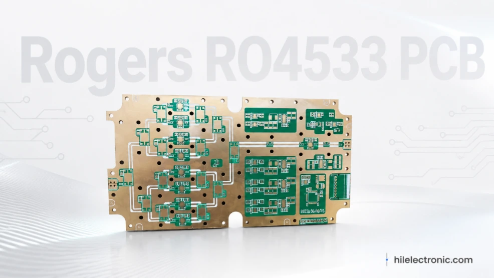
Rogers RO4533 PCB Manufacturing for Cost-Sensitive RF Products
RO4533 should be handled as a grade-specific commercial RF...
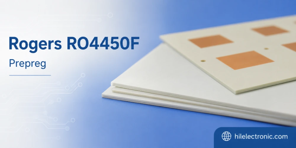
Rogers RO4450F Prepreg for Multilayer RF PCB Manufacturing
“RO4450F prepreg” is not enough information to manufacture...
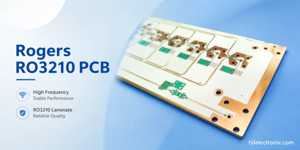
Rogers RO3210 PCB Manufacturing for Extremely Compact RF Circuits
RO3210 is not a routine material upgrade. Rogers publishes...
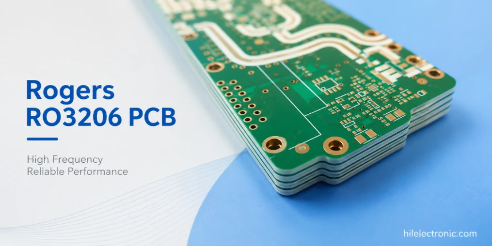
Rogers RO3206 PCB Manufacturing for Miniaturized RF Products
An RO3206 quotation should begin with the dimensions the...
How to get a quote for PCBs
Let‘s run DFM/DFA analysis for you and get back to you with a report. You can upload your files securely through our website. We require the following information in order to give you a quote:
-
- Gerber, ODB++, or .pcb, spec.
- BOM list if you require assembly
- Quantity
- Turn time
In addition to PCB manufacturing, we offer a comprehensive range of electronic services, including PCB design, PCBA, and turnkey solutions. Whether you need help with prototyping, design verification, component sourcing, or mass production, we provide end-to-end support to ensure your project’s success.
For PCBA services, please provide your BOM (Bill of Materials) and any specific assembly instructions. We also offer DFM/DFA analysis to optimize your designs for manufacturability and assembly, ensuring a smooth production process.