
Critical Mistakes in LED Thermal Design and How to Avoid Them

Why LED Thermal Design Determines Success or Failure
LED technology delivers impressive efficiency, yet thermal sensitivity remains its critical vulnerability. Modern LEDs generate substantial heat concentrated in extremely small areas, creating a fundamental challenge for heat management PCB design. When thermal control fails, the consequences cascade rapidly: accelerated light degradation, shortened operational lifespan, and unpredictable reliability failures.
Junction temperatures exceeding design limits trigger exponential phosphor degradation. Color shift becomes visible within months, and failure rates increase dramatically. Understanding common LED thermal design mistakes separates professional-grade products from premature failures.
Common LED Thermal Design Mistakes
1. Underestimating the importance of thermal paths
Many designers focus exclusively on heat sink selection while overlooking the complete thermal pathway from LED junction to ambient air. This fundamental LED heat dissipation oversight creates bottlenecks that no external cooling can overcome. Every interface in the thermal resistance chain adds resistance that accumulates from chip to heat sink.
The thermal path includes LED chip, die attach material, PCB copper layers, dielectric substrate, thermal interface material, and heat sink assembly. Optimizing thermal path design requires systematic attention to every transition point, particularly the PCB stack-up where the most significant temperature drops occur.
2. Use of inappropriate substrate materials
Conventional FR-4 substrates create thermal barriers in high-power LED designs. With thermal conductivity around 0.3 W/mK, FR-4 traps heat near LED junctions. When power densities exceed 1W per LED, junction temperatures rapidly exceed safe limits, triggering accelerated degradation.Metal-core PCB solutions provide the necessary thermal improvement:
- Aluminum core PCBs – Deliver 1-2 W/mK thermal conductivity through standard dielectric layers, suitable for most mid-power applications.
- Advanced IMS configurations – Reach 3-5 W/mK with specialized dielectric materials for high-power LED arrays.
- Copper-core solutions – Offer thermal conductivity exceeding 200 W/mK in the base material for extreme power densities.
The material decision must balance thermal requirements against economic constraints and manufacturing complexity.
3. Improper design of copper thickness and thermal conductive layer
Standard 1 oz copper provides minimal lateral heat spreading, concentrating thermal stress at LED mounting points. This causes solder joint fatigue and temperature gradients that accelerate material degradation.
Increasing copper weight to 2-3 oz significantly improves lateral thermal spreading, distributing heat across larger PCB areas. Strategic copper patterning extends beyond the immediate LED footprint, creating thermal relief zones that reduce peak temperatures while balancing manufacturing cost.
4. Inadequate thermal via design or incorrect placement
Many designs incorporate minimal thermal vias directly beneath LED packages, assuming this addresses heat transfer requirements. This approach fails because via effectiveness depends on density, diameter, plating quality, and spatial distribution. Inadequate thermal vias design creates significant thermal resistance between copper layers.
Effective thermal vias design requires strategic planning:
- Via diameter – Range from 0.3mm to 0.5mm, with smaller diameters enabling higher density placement.
- Optimal spacing – Place vias on 1.0-1.5mm centers within the thermal pad area, extending slightly beyond the LED footprint.
- Via filling – Thermally conductive epoxy filling reduces thermal resistance by 30-50% compared to air-filled vias.
- Via density – Target 15-25 vias per square centimeter in critical thermal zones for high-power applications.
5. Neglecting the selection and installation of thermal interface materials (TIM)
Poor thermal interface material selection creates insurmountable barriers between PCB and heat sink. Low-cost thermal pads with conductivity below 2 W/mK combined with insufficient mounting pressure leave air gaps that dramatically increase thermal resistance.High-performance options each offer distinct advantages:
- Thermal greases – Offer 3-5 W/mK conductivity with minimal bond-line thickness when properly applied.
- Phase-change materials – Provide consistent performance across temperature cycles without pump-out concerns.
- Graphite-based pads – Combine high conductivity with ease of assembly, though at premium cost.
Selection must consider thermal conductivity, long-term stability, assembly process compatibility, and rework requirements.
6. Lack of thermal simulation and test verification
Relying exclusively on past experience without thermal modeling exposes designs to significant risk. Each LED generation delivers higher lumen density with altered thermal characteristics. Previous solutions may fail catastrophically with newer LEDs that concentrate more power in smaller areas.
Thermal simulation identifies potential PCB heat issues before committing to expensive tooling. Even basic finite element analysis reveals hot spots, validates cooling approaches, and quantifies margin against thermal limits. Post-prototype validation using infrared thermal imaging confirms simulation accuracy and exposes manufacturing variations.

Best Practices to Improve LED Thermal Design
Professional thermal design begins during concept development rather than during prototype troubleshooting. Material selection establishes the thermal foundation, with substrate choice driven by power density calculations and target junction temperatures.
Critical design parameters provide starting points:
- Copper weight – Minimum 2 oz for high-power applications with thermal spreading requirements.
- Thermal via density – 15–25 vias per square centimeter in critical zones beneath LED thermal pads.
- Interface materials – Conductivity exceeding 3 W/mK for efficient heat sink coupling.
- Early validation – Thermal analysis before design commitment, followed by prototype testing confirmation.
Implementing these guidelines early reduces redesign cycles, ensures stable junction temperatures, and extends LED lifetime. For projects requiring in-depth thermal simulation, design audits, or material selection support, our engineering team provides customized LED PCB thermal management consulting to accelerate your product’s success.
Partnering with Highleap: Avoiding Common LED Thermal Design Mistakes
Effective LED heat dissipation requires understanding that thermal management extends beyond component selection to system-level engineering. Common LED thermal design mistakes typically arise from oversimplifying this complexity through inappropriate material selection, inadequate thermal spreading, insufficient via implementation, or poor interface management.
Success requires combining proper materials with optimized geometry, validated through simulation and confirmed through testing. This systematic approach transforms heat management PCB design from recurring problems into controlled engineering processes that deliver reliable performance.
At Highleap Electronics, our engineering team specializes in thermal design optimization for demanding LED applications. We offer comprehensive thermal analysis, material selection guidance, and design review services to ensure your LED PCB designs meet performance and reliability targets. Contact us to discuss how our expertise can improve LED PCB heat performance in your next project.

Recommended Posts

RF Transceiver PCB Manufacturing and Assembly
Table of contentsRF Transceiver PCB Manufacturing and...

RFSoC Board PCB Manufacturing and Assembly One-Stop Service
Highleap Electronics supports customer-designed RFSOC...
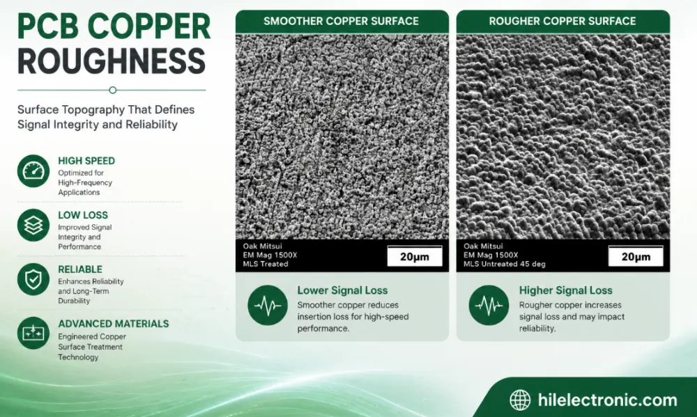
PCB Copper Roughness: Signal Loss, Material Selection and Manufacturing Control
Table of contentsWhat Is PCB Copper Roughness?How Copper...

800G Optical Module PCB Manufacturing and Assembly Service
Table of contentsWhat Makes an 800G Optical Module PCB...
How to get a quote for PCBs
Let‘s run DFM/DFA analysis for you and get back to you with a report. You can upload your files securely through our website. We require the following information in order to give you a quote:
-
- Gerber, ODB++, or .pcb, spec.
- BOM list if you require assembly
- Quantity
- Turn time
In addition to PCB manufacturing, we offer a comprehensive range of electronic services, including PCB design, PCBA, and turnkey solutions. Whether you need help with prototyping, design verification, component sourcing, or mass production, we provide end-to-end support to ensure your project’s success.
For PCBA services, please provide your BOM (Bill of Materials) and any specific assembly instructions. We also offer DFM/DFA analysis to optimize your designs for manufacturability and assembly, ensuring a smooth production process.