
Back to blog
How to Solder BGA components: A Step-by-Step Guide

What is BGA
BGA, or Ball Grid Array, is an advanced type of surface-mount packaging used for integrated circuits (ICs). Unlike traditional pin-grid arrays, BGA packages use an array of tiny solder balls as connectors. These solder balls are arranged in a grid pattern on the underside of the package, directly connecting the IC to the PCB.
BGAs provide superior performance in high-density applications due to their efficient layout, which allows for more connections in a smaller space. This packaging technology is especially beneficial in applications where space is at a premium and high performance is required, such as in mobile devices and laptops.
Why Use BGA Packages
BGA packages are widely used in electronic circuitry for several key reasons. Firstly, their grid-like arrangement of solder balls allows for a higher density of connections, making them ideal for complex, high-pin-count ICs. This density enables more functionality in a smaller space, a crucial factor in miniaturizing electronic devices.
Additionally, BGAs provide better thermal conductivity, allowing for more efficient heat dissipation, which is essential in high-performance electronics. They also offer improved electrical performance due to lower inductance and better signal integrity, making them a preferred choice for high-speed applications.
BGA Soldering Challenges
Alignment and Placement Precision
One of the most critical challenges in soldering BGA components is achieving precise alignment and placement. BGAs have tiny solder balls with very fine pitches, requiring exact alignment with the corresponding pads on the PCB. Even a slight misalignment can lead to incomplete or shorted connections. This necessitates the use of high-precision placement machines and alignment techniques. Proper alignment is crucial not only for establishing a reliable electrical connection but also for ensuring the mechanical stability of the component on the board. Advanced optical systems are often used to align BGAs accurately before the soldering process begins.
Thermal Management
Effective thermal management during BGA soldering is crucial due to the risk of overheating, which can damage the BGA or the PCB. Uneven heat distribution can lead to warping or incomplete soldering, resulting in weak joints. Ensuring a consistent and controlled temperature profile throughout the reflow process is essential. This includes a gradual preheating stage to minimize thermal shock, precise control during the reflow stage to melt the solder evenly, and a controlled cooling phase to solidify the solder joints properly. Advanced reflow ovens with precise temperature control are often used to manage these challenges effectively.
Inspection Difficulties
Inspecting BGA solder joints presents unique challenges due to their structure. Unlike traditional components where solder joints are visible, BGA solder balls are hidden underneath the package. This makes it difficult to visually inspect the quality of the soldering.
To address this, advanced techniques such as X-ray inspection are employed. X-ray inspection allows technicians to see through the BGA package and evaluate the solder joints for issues like voids, bridging, or insufficient solder. This method is non-destructive and crucial for ensuring the reliability of BGA soldering in complex electronics.
Solder Ball Issues
Solder ball issues in BGA soldering arise when solder balls either bridge together or fail to form correctly, leading to potential electrical shorts or open circuits. This can occur due to excessive or insufficient solder paste, incorrect reflow temperatures, or improper handling of components.
To prevent these issues, precise control over solder paste application is essential. Additionally, accurate reflow profiling is necessary to ensure that solder melts and solidifies correctly. Implementing strict quality control measures during both paste application and reflow processes is critical to minimizing the occurrence of solder ball issues in BGA assembly.
Solder BGA Components Process
Applying Solder Paste
The application of solder paste in BGA soldering is a critical step that requires precision. A stencil, specifically designed for the PCB layout, is used to apply the solder paste accurately to the PCB pads. This stencil ensures that the right amount of solder paste is deposited, which is crucial for forming strong and reliable solder joints. The solder paste typically contains tiny balls of solder and a flux mixture, which helps in the proper reflow and bonding of the solder balls on the BGA component to the PCB pads during the reflow soldering process.
BGA Component Placement
BGA component placement is a critical step that requires utmost precision. Specialized pick-and-place machines are used to accurately position BGA components onto the PCB. These machines use optical systems to align the BGA’s solder balls with the corresponding pads on the PCB. The precision of this alignment is crucial because even a slight misalignment can lead to improper connections or short-circuiting. The process also involves careful handling of the components to avoid any damage to the solder balls, ensuring a reliable solder joint during the reflow process.
Reflow Soldering
Reflow soldering is a critical step in the BGA component soldering process. During this phase, the entire assembly – PCB with applied solder paste and precisely placed BGA components – is subjected to controlled heating in a reflow oven. The oven gradually ramps up the temperature to melt the solder paste without damaging the components. This melting creates the necessary solder joints between the BGA’s solder balls and the PCB’s pads. The key to successful reflow soldering is maintaining an accurate temperature profile, which ensures uniform heating and cooling, preventing issues like solder ball deformation or incomplete soldering.
Controlling the Temperature Profile
Controlling the temperature profile during reflow soldering is a critical aspect of the BGA soldering process. The profile typically includes preheating, soaking, reflow, and cooling stages, each requiring precise temperature control to ensure optimal soldering. Preheating gradually raises the PCB’s temperature to avoid thermal shock, while soaking allows heat to permeate the entire assembly evenly. The reflow phase melts the solder paste, forming joints between the BGA components and the PCB. Finally, controlled cooling solidifies the solder without inducing stress. Proper management of this profile is essential to avoid defects like cold joints, voids, or overheating, which can compromise the integrity of the solder joints.
Inspection
After soldering, BGA components require meticulous inspection due to their hidden solder joints. Advanced techniques such as X-ray inspection are commonly used to see beneath the BGA package and evaluate the solder connections. This inspection checks for issues like solder bridging, voids, or insufficient soldering, ensuring each connection meets quality standards. In some cases, automated optical inspection (AOI) can also be employed for surface-level inspection. This phase is crucial for ensuring the reliability and functionality of the assembled PCB.
Rework
Identifying Defects
Identifying defects in BGA soldering is crucial for determining the need for rework. Common defects include solder bridging, voids, or insufficient solder leading to weak joints. Advanced inspection techniques, such as X-ray imaging, are typically used for this purpose, as they allow for a detailed view of the solder joints beneath the BGA package, which are not visible to the naked eye. X-ray inspection helps in detecting internal defects by providing a clear image of the solder connections, enabling technicians to pinpoint specific issues that require rework.
Removing BGA Components
Removing BGA components from a PCB requires precision and care. This process typically involves using a hot-air rework station or an infrared soldering system. The equipment is used to uniformly heat the BGA component to the solder’s melting point, ensuring that the entire component is heated without overheating any specific area. Once the solder is molten, the component can be gently lifted off the board. It’s crucial during this process to maintain the integrity of the PCB, avoiding damage to the pads or traces. Proper heat shielding is also necessary to protect other nearby components from excessive heat exposure.
The Growing Demand for BGA in High-Performance Electronics
Ball Grid Array (BGA) packaging is becoming increasingly popular in high-performance electronics, particularly in industries where small form factor and exceptional performance are critical. With the demand for smaller, more efficient devices rising, BGA technology offers a compact yet highly effective solution for integrating complex circuits. BGAs are used in a wide range of applications, including mobile phones, laptops, gaming consoles, and high-speed networking equipment.
In mobile devices, BGAs enable the integration of high-pin-count processors and memory chips, which are necessary for powering modern smartphones and tablets. Their ability to efficiently handle thermal dissipation makes them ideal for compact devices where space and heat management are at a premium.
Furthermore, with the growth of industries like 5G, artificial intelligence, and autonomous vehicles, BGA’s high-speed signal integrity and thermal management properties are increasingly in demand. As technology evolves, the ability of BGAs to support these advancements makes them an indispensable component in the production of high-performance electronics.
How to Improve Your PCB Assembly with BGA Technology
Incorporating BGA technology into your PCB assembly process offers several advantages, especially when designing and manufacturing complex, high-performance electronics. BGAs enable higher pin counts in a smaller space, reducing the footprint of your PCB while maintaining superior electrical performance and thermal management.
One of the biggest benefits of using BGAs in PCB assembly is the ability to achieve a more efficient layout, allowing for more components in a smaller area. This is particularly beneficial for consumer electronics, where compact design is essential. The use of BGAs also reduces the risk of signal degradation and ensures that components can handle high-frequency signals with greater reliability.
Additionally, BGAs contribute to better heat dissipation compared to traditional pin-based packages. This is crucial for devices that generate a lot of heat, like graphics cards or high-performance processors. Properly soldered BGA connections also help maintain the integrity of the device over time, ensuring that components stay securely attached to the board despite thermal cycling and mechanical stress.
To optimize your PCB assembly with BGA technology, it’s essential to ensure precise placement and accurate soldering. Employing advanced techniques such as X-ray inspection and using high-quality reflow soldering equipment can help ensure that each BGA component is properly placed and soldered, reducing the chances of defects or failures in the final product.
Conclusion
Soldering BGA components requires meticulous attention to detail, a thorough understanding of the soldering process, and the right equipment. From applying solder paste to inspecting and potentially reworking the soldered PCBs, each step is crucial for the functionality and reliability of the final product. Mastering BGA soldering techniques not only ensures high-quality PCB assemblies but also enhances the overall performance of electronic devices.
At Highleap Electronics, we specialize in high-precision PCB manufacturing and assembly services, including expert BGA soldering. With our advanced equipment, in-depth industry knowledge, and commitment to quality, we ensure that your PCBs meet the highest standards of performance and reliability. Whether you’re looking for rapid prototyping or large-scale production, our team is equipped to handle your needs and deliver exceptional results. Partner with us today to bring your electronic designs to life with the highest quality PCB assembly solutions.

Recommended Posts
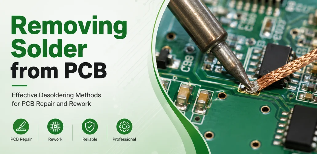
Removing Solder From a PCB Without Pad Damage
Figure 1. removing solder from PCB Removing solder,...
PCB Cleaning After Soldering: Residue and Methods
Figure 1. PCB cleaning contamination and failure risk...
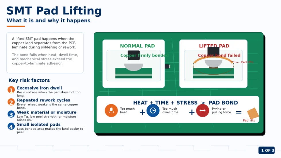
Why SMT Pads Lift During Soldering
Figure 1. SMT pad lifting what it is and why it happens...
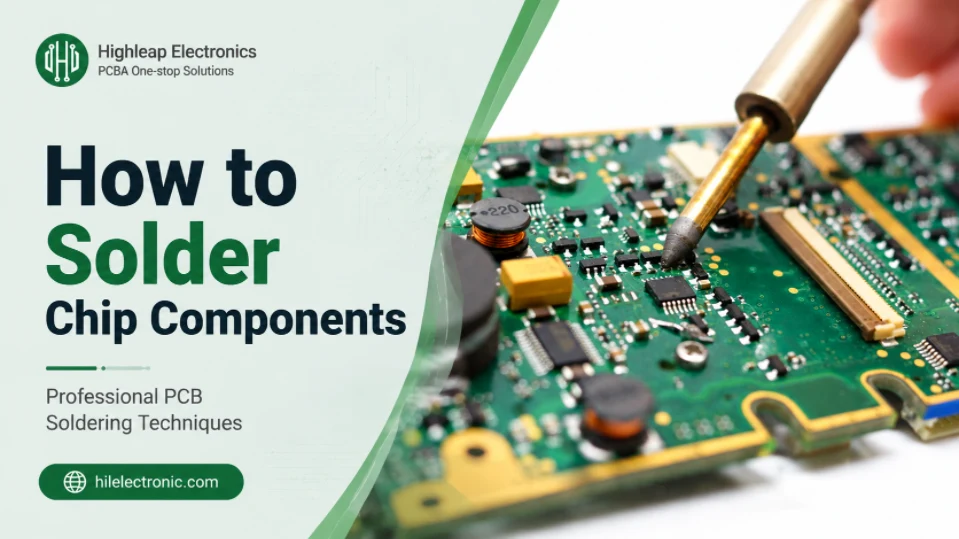
How to Solder Chip Components: SMD Rework Guide
Figure 1. how to solder chip components guide...
How to get a quote for PCBs
Let us run DFM/DFA analysis for you and get back to you with a report.
You can upload your files securely through our website.
We require the following information in order to give you a quote:
-
- Gerber, ODB++, or .pcb, spec.
- BOM list if you require assembly
- Quantity
- Turn time
In addition to PCB manufacturing, we offer a comprehensive range of electronic services, including PCB design, PCBA (Printed Circuit Board Assembly), and turnkey solutions. Whether you need help with prototyping, design verification, component sourcing, or mass production, we provide end-to-end support to ensure your project’s success. For PCBA services, please provide your BOM (Bill of Materials) and any specific assembly instructions. We also offer DFM/DFA analysis to optimize your designs for manufacturability and assembly, ensuring a smooth production process.