
Audio Amplifier PCB: Design Guide, Layout Tips & Assembly | Highleap

An audio amplifier PCB is the physical foundation of every high-fidelity sound system. Whether you are developing a Class AB home stereo, a Class D car audio board, or a professional studio power amplifier, the printed circuit board determines how cleanly the signal is amplified, how much noise is introduced, and how reliably the product survives thousands of operating hours.
This guide covers everything engineers and procurement teams need to know: how an audio amplifier PCB works, the critical design decisions that separate a quiet build from a noisy one, material and layer stack choices, PCB assembly considerations, and how to work with a manufacturing partner who understands amplifier-specific requirements.
What Is an Audio Amplifier PCB?
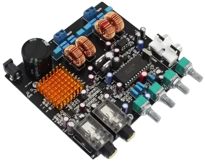
An audio amplifier PCB — sometimes called an amplifier PCB or PCB amplifier board — is a printed circuit board designed to host and interconnect the components that amplify weak audio signals into levels capable of driving loudspeakers, headphones, or recording equipment.
The board carries transistors, MOSFETs, integrated circuits, capacitors, resistors, and power supply components. Its copper traces route signals, power, and ground in a layout that directly determines noise floor, total harmonic distortion (THD), thermal stability, and long-term reliability. Unlike a generic digital PCB, an audio PCB must maintain signal fidelity across the entire audible range — 20 Hz to 20 kHz — while simultaneously handling high currents in the power stage. For a broader look at how these design principles apply across amplifier types, see our overview of amplifier PCB design.
Key Functions of an Audio Amplifier PCB
- Signal amplification: Boosts microphone, instrument, or line-level input signals to speaker-driving output levels.
- Noise isolation: Separates sensitive analog input stages from high-current power stages to prevent interference.
- Power distribution: Delivers stable, filtered DC power to each gain stage without voltage droop or ripple.
- Thermal management: Dissipates heat from power transistors and MOSFETs to protect components and maintain bias stability.
- Protection: Integrates overcurrent, overvoltage, and thermal-shutdown circuitry to safeguard the system.

Amplifier Classes and Their Impact on PCB Design
The amplifier class you choose has a direct influence on PCB layout, copper weight, layer count, and thermal management requirements. Understanding these trade-offs early saves costly re-spins later.
Class A
Class A amplifiers bias the output transistors to conduct for the full 360° of the signal cycle. The result is extremely low distortion and a smooth sound. The downside is low efficiency — typically 15–30% — which means significant heat generation. PCB layouts for Class A designs require robust thermal management: large copper pours, thermal vias, and external heatsinks. Board area is typically larger, and power supply filtering must be excellent to prevent hum.
Class AB
Class AB is the most widely used topology in hi-fi and professional audio. Output transistors conduct slightly more than 180° each, eliminating crossover distortion while achieving higher efficiency (50–70%) than Class A. PCB audio amplifier layouts for Class AB designs must manage matched transistor pairs carefully — thermal coupling between complementary devices is critical for bias stability and low distortion. Our dedicated guide on power amplifier PCB design covers Class AB layout rules in more detail.
Class D
Class D switching amplifiers achieve efficiency of 85–95% by rapidly switching output transistors. This makes them ideal for car audio, portable speakers, and high-density professional systems. However, the switching node generates high-frequency harmonics that can couple into sensitive analog input stages. Class D amplifier PCB layout is among the most demanding: output filter inductors must be shielded, bootstrap capacitors must sit within 5 mm of high-side drivers, and switching signal traces must be physically separated from audio signal paths with a ground plane layer between them.
Amplifier Class Comparison
| Class | Efficiency | Distortion | PCB Complexity | Typical Application |
|---|---|---|---|---|
| Class A | 15–30% | Very low | High thermal area | Hi-fi, studio monitors |
| Class AB | 50–70% | Low | Moderate | Home audio, pro audio |
| Class D | 85–95% | Low (with good layout) | High EMI management | Car audio, portable, PA |
Audio Amplifier PCB Layout: Critical Design Rules
PCB layout is where most audio amplifier performance problems originate. A circuit that simulates perfectly can fail in hardware if layout rules are ignored. A thorough understanding of how to design a PCB layout is the starting point for any amplifier project. The following principles apply to virtually every audio amplifier PCB design.
1. Separate Signal Zones
Partition the board into clear zones: input/preamp stage, power amplification stage, and power supply section. Never route high-current power-stage traces across or near the sensitive input stage. Even a few millivolts of crosstalk from power traces into the input stage will be audible as hum or distortion.
2. Star Grounding
Ground loops are the most common cause of audible hum in audio systems. Implement a star-ground topology where all ground connections — input stage, output stage, power supply, and load return — converge at a single point. This prevents high-current return paths from flowing under sensitive signal traces. For multi-layer amplifier PCB designs, use a dedicated ground plane but carefully manage where different ground domains connect to it.
3. Minimize Signal Trace Length
Keep audio signal traces short and direct. Long traces act as antennas, picking up electromagnetic interference from the power supply and output stage. Route critical input traces away from transformer leads, power supply inductors, and Class D switching nodes. Where signal traces must cross power domains, cross them at 90° with a ground plane layer in between.
4. Decoupling and Bypass Capacitors
Place decoupling capacitors as close as physically possible to the power supply pins of every IC and transistor. For audio ICs, use a combination of electrolytic capacitors for bulk filtering and ceramic capacitors for high-frequency decoupling. Poor decoupling is a frequent cause of supply noise that appears as distortion or oscillation in the output signal.
5. Differential Routing for Signal Pairs
For balanced audio connections — XLR inputs and outputs — route differential signal pairs together with matched trace lengths and consistent spacing. This maintains common-mode rejection across the full audible bandwidth and reduces susceptibility to electromagnetic interference, which is critical in professional audio PCB assembly for studio and live sound equipment.
6. Power and Ground Plane Design
Use solid, uninterrupted power and ground planes rather than routed traces for power distribution. Wide, low-impedance power paths reduce voltage droop under dynamic load conditions — a major source of intermodulation distortion in power amplifiers. For Class D designs, the power plane must be carefully partitioned to prevent switching-frequency noise from coupling back into the audio path.
Component Selection for High-Performance Audio Amplifier PCBs
Component choices directly determine the noise floor, distortion floor, and long-term reliability of an audio amplifier PCB. Cutting corners on component quality is one of the fastest ways to degrade audio performance.
Transistors and MOSFETs
Bipolar junction transistors (BJTs) offer high current gain and are the traditional choice for Class AB output stages due to their predictable gain characteristics. MOSFETs provide higher input impedance and are favored in Class D designs for their fast switching. For matched output pairs in Class AB stages, select devices from the same manufacturing batch or use pre-matched transistor sets to ensure symmetrical crossover behavior.
Capacitors
Film capacitors — polyester and polypropylene types — are preferred for signal coupling and feedback network positions due to their low distortion and stable capacitance over frequency. Electrolytic capacitors are used for power supply filtering and DC-blocking applications; specify low-ESR types rated for at least 105°C. For high-frequency bypass applications near ICs, X7R or C0G ceramic capacitors provide stable characteristics across temperature.
Resistors
Use metal-film resistors with 1% tolerance or better for all gain-setting, feedback, and biasing positions. Carbon composition resistors introduce additional noise and are not appropriate for sensitive input stages. Precision resistors in the feedback network directly determine gain accuracy and distortion floor.
Op-Amps and Audio ICs
For input and pre-amplifier stages, select op-amps specified for audio applications with low voltage noise density — below 10 nV/√Hz — and low THD+N. Popular choices include the NE5532, OPA2134, and LME49720 series. Mark these devices as no-substitute in your bill of materials: seemingly equivalent parts can introduce measurable differences in noise floor and distortion.
PCB Materials for Audio Amplifier Applications
Material selection affects thermal performance, dimensional stability, and dielectric losses at the upper edge of the audio band.
FR4 — The Standard Choice
FR4 glass-epoxy laminate is suitable for the vast majority of audio amplifier PCB designs. It provides adequate thermal resistance, reliable insulation, and cost-effective manufacturability. FR4 is the correct choice for Class AB and most Class D audio amplifier boards operating up to a few hundred watts.
Aluminum-Base PCBs for High-Power Designs
When power dissipation exceeds the capacity of FR4 copper planes and thermal vias, aluminum-base substrates provide direct heat extraction from power devices to the metal core. Thermal conductivity values of 1.0–2.0 W/m·K — compared to 0.3 W/m·K for FR4 — significantly reduce junction temperatures in power transistors and MOSFETs, improving bias stability and extending component lifespan. This is the preferred construction for high-power Class A and professional touring amplifiers. Our detailed guide to aluminum audio amplifier PCB thermal design covers dielectric selection, copper weight optimization, and surface finish choices for metal-core constructions.
Copper Weight Selection
1 oz copper is standard for signal traces. Power amplifier output stages and power supply traces should use 2 oz or 3 oz copper to handle high currents without resistive heating. For output stages carrying sustained currents above 10A, heavy copper PCB design techniques — using 3 oz to 6 oz copper on power layers — provide the current capacity, thermal spreading, and mechanical robustness needed for reliable long-term operation. Specify copper weight clearly in your fabrication notes; inadequate copper on power traces is a common cause of thermal failures in high-power audio amplifiers.
Layer Stack Recommendations
The number of PCB layers affects ground plane integrity, signal isolation, and manufacturing cost.
- 2-layer boards: Suitable for low- to mid-power Class AB designs where board area is available for adequate separation of signal and power zones. Requires careful routing discipline to maintain ground return paths.
- 4-layer boards: The recommended minimum for Class D designs and any application requiring controlled impedance. Dedicate Layer 2 as a solid ground plane and Layer 3 as a power plane, with signal routing on Layers 1 and 4. This configuration provides excellent EMI containment and dramatically improves signal integrity.
- 6-layer and above: Required for complex mixed-signal designs combining analog audio, digital signal processing, and power management on a single board. Allows full separation of analog ground, digital ground, and power distribution networks.
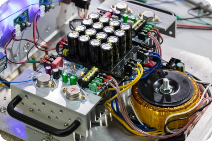
Thermal Management in Audio Amplifier PCB Design
Heat is the enemy of audio quality and component longevity. Every 10°C rise in junction temperature roughly halves the expected lifespan of semiconductor devices. In Class AB output stages, thermal drift causes bias point shifts that manifest as increased harmonic distortion and reduced linearity.
The power supply section deserves particular attention here. A well-designed power supply circuit board with adequate filtering and low output impedance prevents supply-rail noise from entering the audio path and reduces the thermal burden on output stage components. Effective thermal management for audio amplifier PCBs also includes:
- Thermal vias: Arrays of small vias under power device pads conduct heat from the top copper layer to inner planes and the board bottom, reducing thermal resistance between the device and the heatsink.
- Copper pours: Large copper areas connected to device thermal pads spread heat laterally and reduce peak temperatures.
- Component placement: Place heat-generating output transistors away from temperature-sensitive components such as bias adjustment networks and electrolytic capacitors.
- Heatsink coordination: For TO-220 and TO-247 package power devices, board layout must accommodate heatsink mounting hardware and maintain adequate creepage distances.
- Thermal simulation: For designs above 100W, perform thermal simulation before fabrication to identify hotspots and validate that component temperatures remain within datasheet limits under worst-case load conditions.
Audio PCB Assembly: What Defines a Quality Build
Even a perfectly designed audio amplifier PCB will fail to meet its performance specification if assembly process controls are inadequate. Audio amplifiers are sensitive to manufacturing variation in ways that purely digital boards are not — small changes in solder joint resistance, contamination on high-impedance input nodes, or inconsistent thermal pad contact can measurably shift the noise floor, distortion characteristics, or thermal performance. For a comprehensive look at production-specific requirements, our guide on audio amplifier PCB assembly for low noise and yield addresses BOM stability, process controls, and validation strategies in detail.
SMT and THT Process Mix
Most modern audio PCB assembly combines surface mount technology (SMT) for signal processing ICs and small passives with through-hole technology (THT) for high-current output connectors, large filter capacitors, and mechanically stressed components such as potentiometers and binding posts. Define clearly in your assembly specification which components are SMT and which are THT, and specify any mixed-assembly sequences.
Thermal Pad and Power Device Attachment
Power transistors and MOSFETs with exposed thermal pads require careful solder paste stencil aperture design to minimize voiding. Solder voiding under thermal pads is not only a thermal reliability risk — in audio amplifiers, increased thermal resistance causes bias point temperature drift, which increases distortion under sustained load. X-ray inspection of thermal pad solder joints should be specified for Class D and high-power Class AB designs.
Cleanliness of High-Impedance Nodes
Flux residues on high-impedance input traces — op-amp inputs, bias networks, feedback resistors — can introduce resistive leakage paths that shift operating points and increase noise. Specify no-clean flux for audio boards or require post-assembly cleaning with the appropriate solvent system. This is a commonly overlooked cause of hum and noise in assembled audio amplifiers.
BOM Discipline for Audio Performance
Designate noise-critical components — low-noise op-amps, feedback network resistors, film signal capacitors, and audio-grade electrolytic capacitors — as no-alternate or engineer-approved-only in your bill of materials. Footprint-compatible substitutions in these positions can measurably degrade THD+N, noise floor, and long-term stability. Audio performance does not tolerate the same BOM flexibility acceptable in purely functional digital assemblies.
Testing and Validation
Define measurable pass/fail criteria before production begins: noise floor (dBV), THD+N at rated power, frequency response limits, and output impedance. Perform in-circuit testing to verify DC operating points — incorrect bias currents are best caught at board level rather than in system test. For professional audio equipment, include a burn-in soak at rated power to screen for infant-mortality failures in electrolytic capacitors and semiconductor junctions.
Audio Amplifier PCB Applications
PCB amplifier boards appear across a wide range of consumer, professional, and industrial applications:
- Home audio systems: Integrated amplifiers, power amplifiers, AV receivers — typically Class AB with 50W to 500W output power per channel.
- Car audio: Compact, high-efficiency Class D amplifiers designed for 12V supply rails, subject to vibration, temperature extremes, and vehicle EMI environments.
- Professional sound reinforcement: High-power touring amplifiers, installed sound systems, and stage monitors requiring robust construction, comprehensive protection circuits, and reliable performance under continuous duty cycles.
- Guitar and instrument amplifiers: Often use Class AB designs with vacuum tube preamp stages driving solid-state power sections, requiring very low distortion at clean settings and controlled harmonic distortion at driven settings.
- Studio monitors and reference speakers: Demanding Class AB or Class D designs with extremely flat frequency response, low THD, and consistent performance across the full audible bandwidth. For detailed guidance on designing for this application, see our article on designing audio PCBs for quality sound performance.
- Bluetooth speakers and portable audio: Compact Class D PCB audio amplifier designs integrated with Bluetooth SoCs, battery management, and DSP processing. Our guide to Bluetooth speaker PCB design covers the integration considerations specific to wireless audio products.
- RF and wireless applications: Some amplifier designs span the boundary between audio and RF signal processing. Our overview of RF amplifier PCB design addresses the additional impedance matching, material, and EMC requirements that apply when signal frequencies extend above the audio band.
Common Audio Amplifier PCB Design Mistakes to Avoid
Understanding what goes wrong in practice is as valuable as knowing the correct design rules. These are the most frequent mistakes encountered in audio amplifier PCB design:
- Shared ground return paths: Routing high-current output stage return currents through the same copper as the input stage ground causes measurable hum and noise. Always use star grounding or carefully partitioned ground planes.
- Long input traces near power lines: Even a few centimeters of unshielded input trace running parallel to a power supply trace can couple 50/60 Hz hum into the signal.
- Inadequate supply decoupling: Missing or under-specified bypass capacitors allow power supply noise and switching transients to appear in the audio output as distortion or high-frequency hash.
- Ignoring PCB layout for Class D: Treating a Class D amplifier as a simple digital design and ignoring RF containment produces boards that fail EMC testing and inject audible switching noise into the audio output.
- Poor thermal pad contact: Incorrectly fitted or voided thermal pads cause power transistors to run at elevated temperatures, shifting bias points and accelerating aging.
- Floating op-amp inputs: Unused op-amp inputs left floating in multi-channel designs can oscillate and couple interference into active channels. Connect unused inputs to the appropriate reference level via a resistor.
- Undersized copper for power traces: Using 1 oz copper for high-current power supply traces causes resistive heating, voltage drop under load, and can be a fire hazard in high-power designs. Calculate trace current capacity using IPC-2221 guidelines and upsize accordingly — or consider heavy copper construction for sustained high-current paths.
How to Choose an Audio Amplifier PCB Manufacturer
Not all PCB manufacturers and assembly houses are equally equipped to handle audio amplifier PCB production. Amplifier boards have requirements that differ meaningfully from standard digital PCB production:
- Copper weight capability: Confirm the manufacturer can produce 2 oz and 3 oz copper layers without compromising fine-pitch signal trace resolution.
- Aluminum PCB fabrication: For high-power designs, verify the manufacturer has specialized drilling, routing, and surface finish processes for metal-core substrates.
- Controlled impedance: For Class D designs with digital audio interfaces, verify the manufacturer offers controlled impedance fabrication with confirmed dielectric constant values.
- Assembly process discipline: Ask about no-clean versus cleaned flux processes, X-ray inspection capability for thermal pad joints, and BOM change-control procedures.
- Testing capability: Inquire about in-circuit test (ICT), functional audio test fixtures, and burn-in capacity to support your quality requirements.
- Prototyping to production continuity: A manufacturer that handles both prototype and production runs on the same process lines reduces risk when scaling from engineering builds to volume production.
Frequently Asked Questions
What is the difference between a PCB amplifier and a standard PCB?
A PCB amplifier is designed specifically to handle analog signal amplification, which requires stricter attention to noise, grounding, thermal management, and component quality than typical digital PCBs. Signal integrity requirements are tighter, power levels are often higher, and assembly process controls are more demanding.
How many layers does an audio amplifier PCB need?
Low- to mid-power Class AB designs can use 2-layer boards with careful layout. Class D amplifiers and any design with digital signal processing should use 4 layers as a minimum, with dedicated ground and power planes on inner layers. Complex mixed-signal audio processor boards often use 6 or more layers.
What PCB material is best for audio amplifier applications?
FR4 is the correct choice for most audio amplifier PCB designs. High-power amplifiers generating substantial heat benefit from aluminum-base (MCPCB) construction, which provides thermal conductivity values up to six times higher than FR4, reducing junction temperatures and improving long-term reliability.
What causes hum in an assembled audio amplifier PCB?
Audible hum is most frequently caused by ground loops, inadequate star grounding, long unshielded input traces running near power supply components, or flux contamination on high-impedance input nodes. In most cases the root cause is a layout error that can be identified by systematically lifting ground connections and observing which change reduces the hum.
What is the typical copper weight for an audio amplifier PCB?
Signal traces use 1 oz copper. Power output traces, power supply rails, and ground planes in high-current designs should be specified at 2 oz or 3 oz copper to handle rated current without excessive temperature rise or resistive voltage drop.
Can Highleap handle both fabrication and assembly for audio amplifier PCBs?
Yes. Highleap Electronic offers integrated PCB fabrication and assembly services for audio amplifier PCB projects, from prototype to volume production. Our capabilities include FR4 and aluminum-base substrates, controlled impedance fabrication, SMT and THT assembly, and functional test support. Contact us to discuss your project specifications and receive a quotation.
Conclusion
Designing a high-performance audio amplifier PCB requires coordinating layout rules, material choices, component selection, and assembly process controls into a coherent whole. The difference between a clean, low-noise amplifier and one plagued by hum, distortion, or thermal instability is almost always traceable to decisions made at the PCB design and assembly stage — not to the schematic.
Whether you are developing a new PCB audio amplifier product or scaling an existing design to volume production, working with a manufacturing partner who understands the specific demands of audio amplifier boards is one of the most reliable ways to protect audio performance across production builds. Contact the Highleap team to discuss your requirements and get a competitive quote.

Related Articles

Professional Robotics PCB Assembly and Box Build Support
Professional robotics PCB assembly and box-build support. Reliable procurement, precision soldering, and test coverage for scalable production.
TU-865 PCB Material: Complete Engineering Guide for High-Reliability Applications
Complete TU-865 PCB material guide covering Tg 200°C specifications, design considerations, manufacturing processes, and application comparisons for engineers.
TU-768 PCB Material: Specifications, Performance & Practical Design Guide
Complete TU-768 PCB material guide covering technical specs, thermal performance, design tips & application cases. Ideal for engineers selecting high-Tg FR-4 substrates.