
How Does Clone PCB Work and its Benefits

What Is Clone PCB?
Clone PCB, also known as PCB duplication, is the process of reproducing an existing printed circuit board through reverse engineering. Instead of designing from scratch, engineers can replicate the exact layout and functionality of a PCB, saving time and reducing costs. The clone PCB process is widely used to create multiple copies for testing, reproduce outdated or unavailable boards, and adapt proven designs for new projects. This guide explains what clone PCB is, how it works, and the key benefits of using cloning services in electronics manufacturing.
Why You Need Clone PCB Services and Their Benefits
Clone PCB services provide a cost-effective way to reproduce existing designs without going through a lengthy design cycle. Whether you need multiple boards for product testing, customer samples, or preparation for mass production, PCB duplication ensures you can generate boards quickly and reliably. If your design is outdated or no longer available, clone PCB techniques help recreate and improve it for modern use.
Core Benefits of Clone PCB
- Making modifications or improvements to the original design
- Creating multiple copies for mass production
- Producing an identical copy of an existing electronic product
- Adapting an existing PCB design with modifications
- Developing a PCB from a design
- Creating a backup if the original is lost or damaged
- Testing a design before full-scale manufacturing
- Repairing damaged tracks
- Replacing missing electronic components
Additional Benefits of PCB Cloning
- Optimizes Time and Cost: Cloning PCB is more efficient compared to traditional PCB manufacturing, saving both time and money. You avoid the lengthy design process and reduce costs related to PCB testing and prototyping, as the original design is already established.
- Simplifies Production: The production process becomes more straightforward as manufacturers can reverse engineer innovative designs. The automated cloning process streamlines production, automating manufacturing processes and saving on manual labor costs. This leads to the production of high-performance, long-lasting boards.
- Improved Scalability and Freedom: Cloning PCB offers flexibility to adapt throughout the manufacturing process and to produce boards that meet consumer needs. It also supports scalability, allowing a large number of boards to be manufactured from a single design.
- Building Customer-Friendly Products: Engineers can build products that cater to customer preferences by reverse engineering effective PCB designs.
- Offers Production Flexibility: A single PCB design can be used to mass manufacture products, providing flexibility in production.
- Consistency in Performance: Cloned boards maintain consistency in performance, as the design has been tried and tested.
- Improves Timelines: PCB cloning significantly reduces the time-to-market, providing a competitive edge through its simplicity and speed.
How to Clone PCB: Step-by-Step PCB Cloning Process
Several methods are available for cloning a PCB, each with unique benefits and challenges. Understanding these methods and their potential issues is crucial for making an informed choice and achieving the desired outcome. Generally, the PCB cloning process involves the following steps:
#1 – IC Unlock (Decryption)
Extract the program from the board if it is locked.
#2 – PCB Reverse Engineering
Obtain the Gerber files and BOM list, create the layout, and convert it into a schematic.
#3 – Prototype PCB Fabrication
Produce a sample PCB based on the schematic.
#4 – PCB Functional Testing
Evaluate the performance of the new board, troubleshoot issues, and resolve any incompatibilities before proceeding to mass production.
Tips:
- For #1, IC unlock is only necessary if the program is protected.
- For #2, reverse engineering is crucial for obtaining the BOM and schematic diagrams.
Required Tools and Equipment:
- Computer
- AUTOCAD
- Scanner
- PROTEL
| Cloning Method | Required Tools/Software | Advantages | Limitations |
|---|---|---|---|
| Manual Reverse Engineering | Multimeter, CAD software, schematic capture tools | Low cost, suitable for simple PCBs, flexible for custom modifications | Time-consuming, high risk of errors, not practical for multilayer boards |
| Scanning & CAD Reconstruction | Scanner, AutoCAD, PROTEL/Altium Designer | Accurate reproduction of PCB layout, faster than manual tracing, scalable | Requires skilled engineers, limited by scan resolution for fine-pitch components |
| IC Unlock & Firmware Extraction | IC programmer, decryption tools | Enables full reproduction of hardware and software, useful for system-level cloning | Legal/IP issues, technically complex, sometimes impossible with strong encryption |
| Professional PCB Duplication Services | Reverse engineering equipment, Gerber/BOM generation software | High accuracy, reduced turnaround time, includes testing & prototyping | Higher cost, dependent on service provider expertise |
Clone PCB: Step-by-Step Process
- Scan the Original PCB
Place the original PCB in a scanner and adjust contrast and brightness settings. - Open AUTOCAD and Create a File
Start AUTOCAD, create a new file, and insert raster images of the PCB. Draw a rectangular frame around the PCB and use object lock points for accurate alignment. - Draw Component Packages and Shapes
Design the board by calculating the required quantity. Each package should include one board drawing. Use PROTEL99 to generate component packages and shapes. - Import CAD Files into PROTEL99
Open PROTEL99 PCB editor, select ‘import CAD file’ from the menu, and import the CAD file. You will see the component packaging graph in the PROTEL99 editor. - Create PCB Component Editor
Use PROTEL99’s PCB component editor to open another instance and place components. - Send Component Packages to CAD File
After creating component packages in PROTEL99, export each to a CAD file. - Copy the Component Package to the CAD File
Duplicate the PCB image into the imported CAD file by copying the component packages. Open both CAD files for this task. - Add Vias and Pads
Measure the diameters of the pads and vias, then use the Circle sub-item from the drawing menu to place them accurately. Ensure proper placement and filling in the CAD file. - Draw Traces and Add Silkscreen
Use the Drawing menu to select line aggregates and add the silkscreen. For irregular screens, use the polymer line tool.
Applications of Clone PCB
Clone PCB technology is widely adopted where cost efficiency, product continuity, and reverse engineering PCB solutions are required. Typical use cases of PCB duplication and PCB cloning services include:
- Industrial Control Systems – Reproduce discontinued circuit boards to keep automation equipment running without costly redesigns; extend lifecycle with a reliable clone PCB.
- Consumer Electronics – Duplicate proven layouts to shorten development for smartphones, wearables, and household devices using a structured PCB cloning process.
- Medical Devices – Maintain consistency and compliance by recreating boards for diagnostic equipment; leverage clone PCB for controlled revisions.
- Automotive Electronics – Use PCB duplication to scale and adapt validated designs for ECUs, ADAS modules, and infotainment systems.
- Repair & Maintenance – Clone PCB to replace damaged or obsolete boards, create backups, and support long-term service of legacy products.
By applying clone PCB methods across these industries, engineers can reduce cost, accelerate time-to-market, and sustain reliable performance throughout the product lifecycle.
Conclusion: Key Takeaways of Clone PCB in Electronics Manufacturing
Clone PCB is a valuable solution in modern electronics manufacturing, enabling the duplication of outdated designs, reverse engineering PCB layouts, and improving existing products with proven reliability. While PCB duplication and cloning services involve challenges such as legal considerations and the technical complexity of reverse engineering, the benefits—cost savings, faster production cycles, and consistent performance—make clone PCB an attractive option for engineers and manufacturers. By applying the right tools and a systematic PCB cloning process, companies can streamline development and extend product lifecycles.
FAQ
1. What does it mean to clone PCB?
Cloning PCB, also called PCB duplication, is the process of creating an identical copy of an existing circuit board through reverse engineering and reproduction techniques.
2. Why do engineers or companies need to clone PCB?
Clone PCB services are often used to reproduce outdated boards, reduce design time, repair damaged products, or prepare multiple copies for mass production and testing.
3. Is it legal to clone PCB from an existing design?
The legality of cloning PCB depends on intellectual property rights. If the original design is protected by copyright or patents, permission is required before duplication.
4. What are the benefits of using clone PCB services?
Key benefits include cost savings, faster production, consistency in performance, improved scalability, easier repair of damaged designs, and reduced time-to-market.
5. What tools are required to successfully clone PCB?
Common tools for PCB cloning include CAD software (like AutoCAD), PROTEL, scanners, and computers for generating Gerber files, BOM lists, and schematics.

Recommended Posts
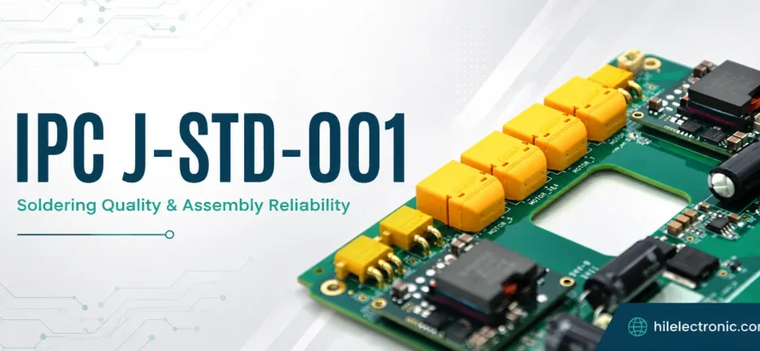
IPC J-STD-001: Classes, Requirements, and RFQ Specification
Figure 1. IPC J-STD-001 image for Highleap Electronics PCB...
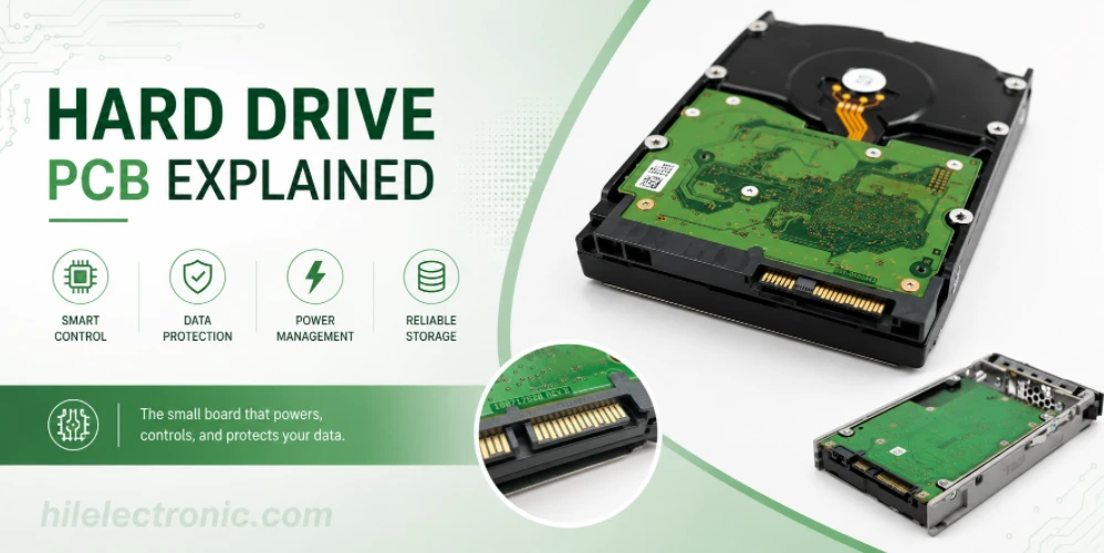
Hard Drive PCB: Function, Failure Modes, and Manufacturing
Figure 1. hard drive PCB image for Highleap Electronics...
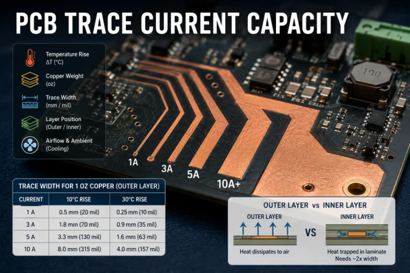
PCB Trace Width Calculator: How to Size Traces for Current, Voltage Drop, and Impedance
Figure 1. A PCB trace width calculator is a starting point...
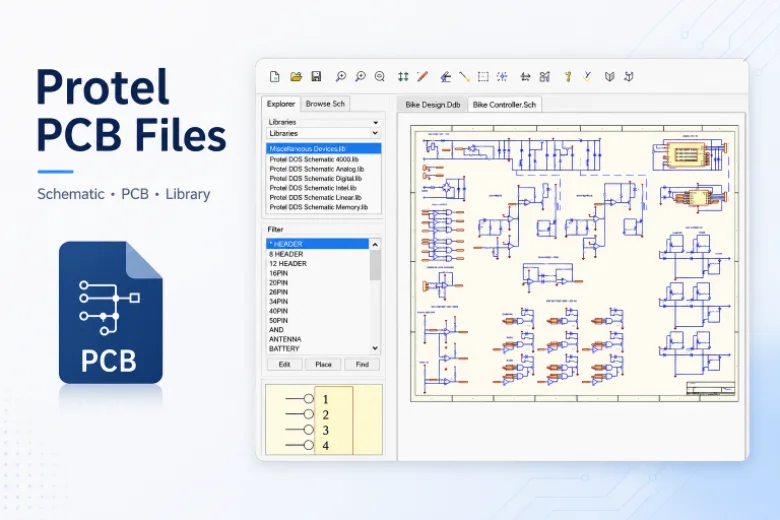
Protel PCB: Is It the Same as Altium Designer, and How to Open Legacy Protel Files
Figure 1. Legacy Protel PCB files often need review before...
How to get a quote for PCBs
Let us run DFM/DFA analysis for you and get back to you with a report.
You can upload your files securely through our website.
We require the following information in order to give you a quote:
-
- Gerber, ODB++, or .pcb, spec.
- BOM list if you require assembly
- Quantity
- Turn time
In addition to PCB manufacturing, we offer a comprehensive range of electronic services, including PCB design, PCBA (Printed Circuit Board Assembly), and turnkey solutions. Whether you need help with prototyping, design verification, component sourcing, or mass production, we provide end-to-end support to ensure your project’s success. For PCBA services, please provide your BOM (Bill of Materials) and any specific assembly instructions. We also offer DFM/DFA analysis to optimize your designs for manufacturability and assembly, ensuring a smooth production process.