
HDI Stackup Design Guide for Production-Ready PCBs

A production-ready HDI stackup is not a “layer count decision.” It is a controlled construction plan that defines how build-up layers, microvias, dielectric thickness, copper build, and reference planes work together to achieve routing density without sacrificing yield, impedance accuracy, or long-term reliability. In high-pin-count BGAs and compact electronics, the stackup is often the main lever that determines whether the program scales smoothly from prototype to volume.
At Highleap Electronics, we engineer HDI stackups using a manufacturing-first approach and a closed-loop workflow across printed circuit board fabrication and electronics assembly (SMT/THT). This helps OEM teams eliminate the most common HDI failure mode: a stack-up that routes well in CAD, but does not hold stable capability in real production (microvia quality, registration, planarity, impedance, and warpage).
Table of Contents
- HDI Stackup Fundamentals: What Must Be Defined to Make It Buildable
- Selecting the Right Build-Up: 1+N+1 vs 2+N+2 vs 3+N+3
- Microvia Engineering: Staggered vs Stacked, Fill Specs, and Reliability Controls
- Controlled Impedance in HDI Stackups: How to Make It Repeatable and Reportable
- DFM for HDI Stackups: The Hidden Drivers of Yield, Warpage, and Total Cost
- What to Send for a Fast, Accurate HDI Quote (RFQ Package That Gets Real Answers)
1) HDI Stackup Fundamentals: What Must Be Defined to Make It Buildable
An HDI stackup becomes “manufacturing-ready” when design intent is translated into parameters that can be measured, controlled, and verified. If your stack-up only lists nominal thicknesses and a target impedance, you are leaving critical variability undefined—and HDI variability will show up in yield, impedance drift, or assembly defects.
- Build-up architecture: Specify whether the board is 1+N+1, 2+N+2, 3+N+3, or any-layer HDI (ELIC), and identify the core structure and sequential lamination count.
- Dielectric thickness ranges (not only nominal): Sequential lamination increases sensitivity to thickness variation; defining acceptable ranges improves deliverability and reduces re-spin risk.
- Copper build model: List base copper and expected plating growth, especially on outer layers where copper build affects trace geometry and impedance.
- Reference planes and return paths: Identify where controlled-impedance traces reference GND/Power planes and ensure plane continuity for stable return current paths.
- Verification intent: Define whether you require impedance coupons, microsection coupons, X-ray, or other validation outputs for lot-to-lot consistency.
If you are unsure how to format these requirements, start by aligning your stackup with your supplier’s DFM window and request a build recommendation from an high-density interconnect PCB manufacturer.
2) Selecting the Right Build-Up: 1+N+1 vs 2+N+2 vs 3+N+3 (Cost, Yield, and Lead Time)
Build-up selection is the primary knob that trades density for process complexity. More build-up layers can reduce board area and simplify routing—but each additional lamination cycle increases registration sensitivity, process variation, and validation requirements. Over-building is one of the most common reasons quotes come back high or schedules slip.
- 1+N+1 (most common for scalable HDI): Best cost/yield balance, fewer lamination cycles, and typically the fastest route to stable mass production for many dense designs.
- 2+N+2 (for tighter BGA escape and compact modules): Improves channel availability and via distribution for fine-pitch BGAs, but requires tighter registration control and more discipline on microvia quality and copper balance.
- 3+N+3 (density-driven, validation-heavy): Maximum routing freedom for aggressive via-in-pad usage and dense I/O, but increased sensitivity to microvia fill quality, lamination integrity, and warpage control.
- Practical engineering rule: Start with the lowest-complexity build-up that meets escape routing and impedance constraints, then use DFM feedback to confirm margins. If DFM drives a change, it is usually cheaper to adjust build-up early than to iterate during prototype builds.
For faster selection and quoting, Highleap can review your design package and recommend a build-up that matches performance goals and real capability windows.

3) Microvia Engineering: Staggered vs Stacked, Fill Specs, and Reliability Controls
Microvias are the defining feature of HDI—and the most common source of reliability variation if under-specified. In practice, “microvia” is not one thing; the outcome depends on via geometry, layer pairing, fill method, plating uniformity, and sequential lamination conditions.
- Prefer staggered microvias where routing allows: Staggered structures typically distribute stress more favorably, making long-term reliability and yield stability easier to maintain in volume.
- Use stacked microvias only when density forces it: Stacked structures increase sensitivity to fill integrity and interconnect quality. If stacked microvias are required, specify fill, planarization expectations, and verification requirements explicitly.
- Define microvia layer pairs: Clearly list which layers use laser vias (e.g., L1–L2, L2–L3) and which vias are through-hole or buried. This prevents misinterpretation and accelerates CAM/DFM.
Via Fill and Planarity (Critical for Via-in-Pad)
- Via-in-pad under BGAs: Specify fill method (e.g., resin plug or copper-filled) and a planarity requirement appropriate for your package pitch and assembly process.
- Acceptance intent: Define whether microsection coupons are required for fill verification and whether X-ray is required for high-risk interconnect zones.
- Why this matters: Under-defined fill specs often show up as rework, inconsistent solder joints, or latent reliability issues—especially under thermal cycling.
If your project is turnkey, a stackup that is “fab-feasible” but not “assembly-robust” will still cost you time. Combining fabrication and assembly under one loop can reduce these risks; see our turnkey PCB assembly service.
4) Controlled Impedance in HDI Stackups: How to Make It Repeatable and Reportable
In HDI, impedance variation can increase because sequential lamination and copper build effects make geometry more sensitive. To prevent “it passed once” outcomes, impedance must be engineered as a controlled deliverable rather than a nominal target.
- State the full impedance definition: Target value, tolerance, single-ended vs differential, and which nets require control.
- Define the structure: Microstrip vs stripline, reference plane assignment, and any constraints on plane splits or return path discontinuities.
- Use thickness ranges and copper build assumptions: Nominal-only stackups are fragile in HDI. Range-based specs improve manufacturability and reduce impedance drift.
- Request coupons when appropriate: Impedance coupons and per-lot test data are the most direct way to keep impedance stable across production lots.
If you need help converting SI requirements into a manufacturing-deliverable stack-up, reference our resource on impedance controlled PCBs.

5) DFM for HDI Stackups: The Hidden Drivers of Yield, Warpage, and Total Cost
HDI programs often suffer cost inflation from “quiet” DFM gaps—details that don’t look dramatic in CAD, but drive scrap, rework, and schedule risk in production. A strong HDI stackup includes DFM rules that protect margins.
- Stackup symmetry for warpage control: Balanced constructions reduce bow/twist risk and improve assembly robustness under large BGAs and tight coplanarity windows.
- Copper balance strategy: Uneven copper distribution can cause resin flow variation during lamination and local thickness changes that impact impedance and planarity.
- Registration margin planning: Capture pads, annular ring targets, and alignment margins should be intentional to avoid marginal yields when running at scale.
- Layer-specific min trace/space: Outer layers behave differently due to plating; inner layers are sensitive to etch and laminate stability. Defining per-layer constraints improves predictable output.
- Design-for-assembly stackup checks: In dense builds, warpage, pad planarity, and solder mask registration interact strongly with BGA yield. It is cheaper to adjust stack-up than to fight assembly defects later.
For customers who need consistent verification, align inspection requirements early. Our overview of PCB inspection and quality control can help you decide what validation outputs to request.
6) What to Send for a Fast, Accurate HDI Quote (RFQ Package That Gets Real Answers)
High-quality inquiries get high-quality quotes. If your RFQ package is complete, you avoid multiple clarification rounds and receive a faster, more accurate price and lead time—along with DFM feedback that highlights true yield risks.
Include These Files
- Gerber or ODB++ (including solder mask, silkscreen, outline)
- Stackup drawing (preferred) or layer count + target thickness
- Impedance table (targets + tolerance + structure)
- Drill + via notes (microvia layer pairs, via-in-pad zones)
Include These Build Requirements
- Build-up type: Specify 1+N+1 / 2+N+2 / 3+N+3 (or request recommendation).
- Via fill requirements: Resin plug vs copper fill, plus planarity requirement for via-in-pad areas.
- Surface finish: ENIG / ENEPIG / OSP (as needed).
- Quantity + delivery target: Prototype vs production volumes.
If You Need PCBA (Recommended for Dense HDI)
- BOM with approved alternates (if available)
- Pick-and-place file (XY)
- Assembly drawing with special process notes
To get started, submit your RFQ here: Get A Quick Quote.
Summary: A scalable HDI stackup is built on deliverable specifications—microvia structure and fill, impedance that is testable, lamination symmetry, and DFM rules that protect yield. When fabrication and assembly feedback are aligned early, you reduce iteration cycles, stabilize quality, and accelerate ramp to volume.

Recommended Posts
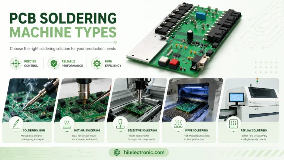
PCB Soldering Machine Types: Reflow, Wave, and Selective Equipment
Figure 1. PCB soldering machine types image for Highleap...
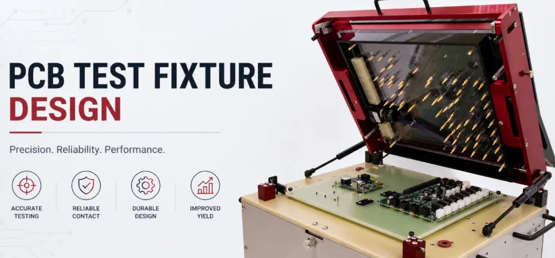
PCB Test Fixture Design: Bed-of-Nails, Flying Probe, and DFT
Figure 1. PCB test fixture design image for Highleap...

Clean Flux vs No-Clean Flux: Residue, Cleaning, and PCB Reliability
Figure 1. clean flux vs no-clean flux image for Highleap...
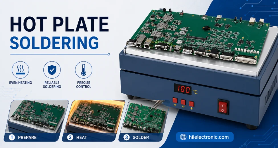
Hot Plate Soldering: Process, Limits, and Reflow Comparison
Figure 1. hot plate soldering image for Highleap...
How to get a quote for PCBs
Let us run DFM/DFA analysis for you and get back to you with a report.
You can upload your files securely through our website.
We require the following information in order to give you a quote:
-
- Gerber, ODB++, or .pcb, spec.
- BOM list if you require assembly
- Quantity
- Turn time
In addition to PCB manufacturing, we offer a comprehensive range of electronic services, including PCB design, PCBA (Printed Circuit Board Assembly), and turnkey solutions. Whether you need help with prototyping, design verification, component sourcing, or mass production, we provide end-to-end support to ensure your project’s success. For PCBA services, please provide your BOM (Bill of Materials) and any specific assembly instructions. We also offer DFM/DFA analysis to optimize your designs for manufacturability and assembly, ensuring a smooth production process.