
Everything You Need to Know About PCB Power Supply Design

Unregulated power supplies are a simple and inexpensive option for converting AC power from a wall outlet to a DC voltage. They typically consist of a transformer to step down the voltage, a rectifier to convert AC to DC, and a filter capacitor to smooth the output. However, since they lack a regulator, the output voltage will have a ripple waveform, which is the AC component superimposed on the DC voltage. This ripple can cause issues in sensitive electronic circuits.
Regulated power supplies, on the other hand, are designed to minimize the ripple and provide a stable DC output voltage. There are two main types of regulated power supplies: linear regulators and switching regulators (also known as switch-mode power supplies).
Challenges and Solutions in Linear Power Supply Design for PCBs
Linear power supply circuits are relatively simple and straightforward to design and implement on a PCB. However, they come with their own set of challenges primarily related to efficiency and heat management. These issues can be particularly challenging when temperature-sensitive components are mounted on the PCB or when the entire assembly is enclosed within an environmentally sealed casing for protection, as cooling options are limited:
- Inefficiency: Linear power supplies are known for their inefficiency. They work by dissipating excess voltage as heat, which results in significant power losses in the form of thermal energy. This inefficiency can lead to higher operating costs and may not be suitable for battery-powered or energy-efficient devices.
- Heat Management: Managing the heat generated by linear power supplies is crucial, especially when temperature-sensitive components are in close proximity. Excessive heat can affect the performance and reliability of these components and may necessitate additional cooling solutions.
- Limited Cooling Options: In some cases, linear power supplies are used in environments where cooling options are limited. For example, if the entire PCB assembly is enclosed within a sealed casing for protection against environmental factors, there may be limited airflow and cooling mechanisms available. This can exacerbate the heat management challenge.
To address these challenges in linear power supply designs, PCB designers must consider several strategies:
- Heat Sinks: Heat sinks can be added to components that tend to get hot, such as voltage regulators. These sinks help dissipate heat more effectively.
- Component Placement: Consider the placement of temperature-sensitive components and heat-generating elements to minimize the impact of thermal interference.
- Thermal Design: Ensure that the PCB layout allows for heat to be conducted away from sensitive areas. This may involve copper pours or heat-conducting vias.
- Environmental Considerations: If the PCB assembly is enclosed, ensure that the casing is designed to facilitate heat dissipation while maintaining environmental protection.
While linear power supplies may be less efficient, they remain a viable choice for certain applications where simplicity, low cost, and stability are essential. Effective heat management is key to ensuring the longevity and reliability of PCBs using linear power supply circuits.

Optimizing PCB Power with Advanced Switch-Mode Power Supplies (SMPS)
Switch-mode power supply (SMPS) circuits are more complex than linear power supplies but offer significantly higher efficiency. While this efficiency is advantageous in terms of thermal management and energy conservation, SMPS designs introduce a new set of challenges for PCB designers. These challenges primarily revolve around managing electromagnetic noise, addressing ripple voltage on the output, and mitigating ground bounce issues:
- Electromagnetic Noise: SMPS circuits have the potential to generate substantial levels of electromagnetic interference (EMI) due to the rapid switching of components. PCB designers must effectively manage this electrical noise to prevent it from affecting other components on the board or interfering with nearby equipment. In some extreme cases, this EMI can even travel back through the mains electricity supply, affecting other devices connected to the same electrical network.
- Ripple Voltage: SMPS circuits can introduce ripple voltage on the output. If not managed correctly, this ripple voltage can induce interference on the PCB. Capacitive or inductive coupling between closely routed traces or bundled wires can exacerbate this issue. Careful PCB layout and filtering techniques are essential to reduce the impact of ripple voltage.
- Ground Bounce: Rapid switching in SMPS circuits can lead to transient changes in the ground potential at the point where the switching components connect to the ground plane on the PCB. This can create a temporary potential difference across the board’s ground plane. In extreme cases, this ground bounce may result in components in distant areas of the PCB detecting and responding to this perceived signal caused by the false potential difference.
To address these challenges and ensure the proper functioning of SMPS designs, PCB designers must implement effective noise suppression, filtering, and grounding techniques. Additionally, minimizing the length and width of high-current loops, employing proper decoupling capacitors, and maintaining a systematic approach to component placement can help reduce EMI and ripple voltage issues. Ground bounce can be mitigated through careful layout and by ensuring low-impedance grounding. Understanding and addressing these SMPS-related challenges are essential for PCB designers working on power supply circuits.
Best Practices for PCB Power Supply Design
When designing the PCB power supply, there are several best practices and considerations that can help ensure power integrity and signal integrity. Here are some key points to keep in mind:
Separate Power and Ground Planes: It is generally recommended to have separate power and ground planes on the PCB. This helps minimize voltage drops, reduces noise coupling between different components, and provides a low impedance path for return currents.
Decoupling Capacitors: Place decoupling capacitors as close as possible to the power pins of each integrated circuit (IC). These capacitors help provide a stable local power supply and reduce the impact of transient currents. Use a combination of ceramic and electrolytic capacitors to cover a wide range of frequencies.
Proper Component Placement: Place the power supply components close to each other to minimize trace lengths and reduce parasitic inductance and resistance. Keep the traces short and direct to minimize voltage drops and noise coupling.
Thermal Considerations: If your power supply circuit generates significant heat, ensure proper thermal management. Use thermal vias, heat sinks, and thermal pads to dissipate heat efficiently. Adequate airflow and ventilation should also be considered.
Grounding Techniques: Implement a solid ground plane and use a star grounding scheme. Connect all ground points directly to the ground plane to minimize ground loops and reduce noise. Separate analog and digital ground regions if necessary, and connect them at a single point.
EMI Filtering: Add appropriate EMI filtering components to suppress conducted and radiated electromagnetic interference. This may include ferrite beads, common-mode chokes, and series inductors on power and signal lines. Carefully design the PCB layout to minimize loop areas and keep noise-sensitive traces away from high-power or high-speed switching circuits.
Shielding: In cases where high current or switching regulators are used, or when there are sensitive nearby circuits, consider adding shielding to the PCB. Metal shielding can help isolate and protect sensitive components from EMI interference.
Test and Validate: Once the PCB design is complete, perform thorough testing and validation of the power supply circuit. Measure the output voltage, ripple, and noise levels under different load conditions to ensure they meet the requirements of your device.
By following these best practices and considering the specific requirements of your power supply design, you can enhance power integrity, minimize noise, and ensure reliable operation of your device.
Conclusion
PCB power supply design is a fundamental aspect of electronic device development, whether it relies on batteries, solar panels, or wall outlets. It extends beyond the basic task of converting AC to DC power, encompassing critical considerations such as power integrity, signal integrity, thermal management, and EMI mitigation. Collaborating with experienced manufacturers like Highleap, a leading PCB&PCBA manufacturer, can be instrumental in achieving these objectives. By selecting the appropriate regulator type, implementing effective thermal management, and employing strategies like bypassing, decoupling, and shielding, designers can ensure that their power supply systems deliver clean, stable power to electronic components, fostering optimal performance and reducing the risk of interference or damage.
In particular, the choice between linear and switching regulators offers a trade-off between low noise and high efficiency. Linear regulators, although quiet, require careful thermal management due to heat dissipation, while switching regulators offer efficiency but require EMI suppression and filtering. Highleap’s expertise in PCB manufacturing and assembly can provide valuable insights and solutions to ensure power integrity and signal integrity while managing thermal considerations, thereby paving the way for robust PCB power supply design and safeguarding the functionality and reliability of electronic devices.
Additional FAQs for PCB Power
- What is the impact of trace width on PCB power delivery?
The trace width directly affects the resistance and current-carrying capacity of the power traces. Wider traces reduce resistance, minimize voltage drops, and improve power distribution, especially in high-current applications. - How do you select the right PCB material for power circuits?
The choice of PCB material depends on thermal conductivity, dielectric constant, and reliability under thermal stress. Materials like FR4 are common for standard power circuits, while advanced materials like Rogers are used for high-frequency or high-power designs. - What role does PCB stack-up play in power supply design?
A well-designed stack-up reduces noise, enhances signal integrity, and provides low-impedance power and ground planes. It is crucial for minimizing EMI and ensuring stable power delivery. - How can ground loops be avoided in PCB power designs?
Ground loops can be avoided by implementing a solid ground plane, using a star grounding scheme, and ensuring all components share a common reference point for the ground. - What testing methods ensure PCB power reliability?
Testing methods include thermal profiling, ripple voltage measurement, EMI testing, and load testing under varying conditions. These tests help validate the design and detect potential issues early. - How do thermal vias improve PCB power performance?
Thermal vias transfer heat from the top layer to internal layers or the bottom of the PCB, enhancing heat dissipation. This is particularly important in high-power designs with limited airflow.

Recommended Posts
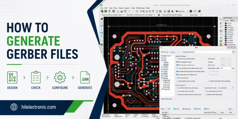
How to Generate Gerber Files for PCB Manufacturing
Figure 1. how to generate Gerber files image for Highleap...
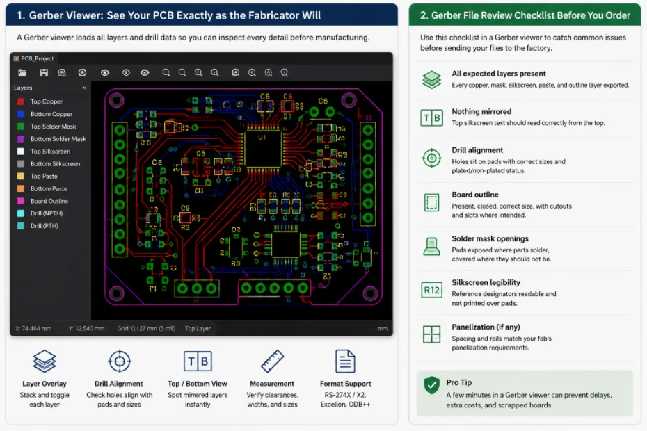
Gerber File Review Checklist: How to Check PCB Files Before You Order
Figure 1. Gerber file review catches missing layers, drill...
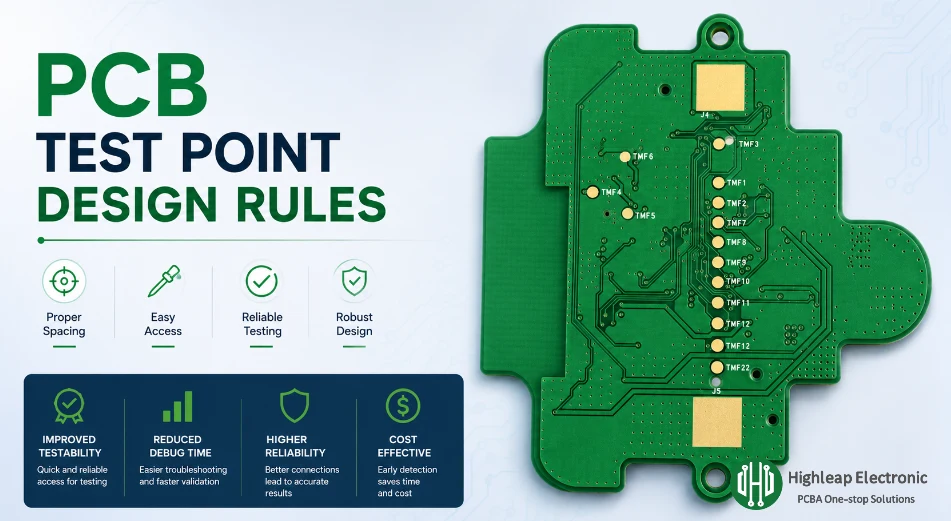
PCB Test Point Design Rules for Debug and ICT
Figure 1. PCB test point design rules help make debugging,...
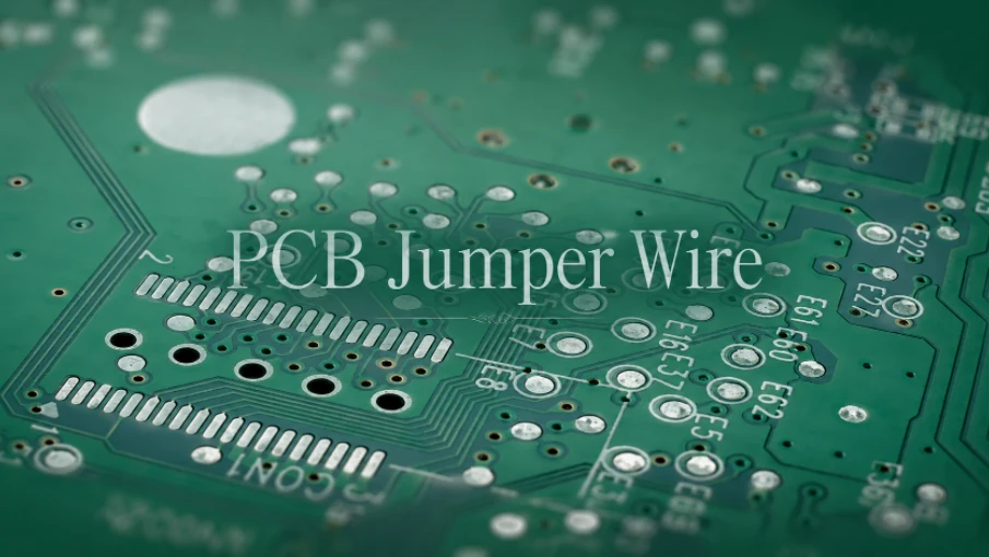
PCB Jumper Wire: Uses, Types, and Design Tips
Figure 1. PCB jumper wires are useful for prototypes and...
How to get a quote for PCBs
Let us run DFM/DFA analysis for you and get back to you with a report.
You can upload your files securely through our website.
We require the following information in order to give you a quote:
-
- Gerber, ODB++, or .pcb, spec.
- BOM list if you require assembly
- Quantity
- Turn time
In addition to PCB manufacturing, we offer a comprehensive range of electronic services, including PCB design, PCBA (Printed Circuit Board Assembly), and turnkey solutions. Whether you need help with prototyping, design verification, component sourcing, or mass production, we provide end-to-end support to ensure your project’s success. For PCBA services, please provide your BOM (Bill of Materials) and any specific assembly instructions. We also offer DFM/DFA analysis to optimize your designs for manufacturability and assembly, ensuring a smooth production process.