
MCPCB Stack-up Design | Key Configurations and Engineering Considerations

Introduction
The MCPCB stack-up represents a critical engineering decision in thermal management applications, determining both heat dissipation efficiency and electrical performance. As power densities in electronic systems continue to increase, the metal core PCB layer structure directly influences how effectively heat transfers from components to ambient environments.
Understanding different MCPCB stack-up configurations enables engineers to balance thermal requirements, electrical isolation, and manufacturing constraints. This technical analysis examines various MCPCB layout architectures, from single-layer to complex multilayer designs, providing engineering insights for optimal stack-up selection and implementation.
What Is MCPCB Stack-up?
Defining Stack-up Architecture
MCPCB stack-up refers to the sequential arrangement of material layers that compose a metal core printed circuit board, defining the thermal and electrical pathways through the structure. This layered configuration typically includes:
- Copper Foil Layer – Forms the circuit layer that carries electrical signals and distributes heat laterally.
- Dielectric Layer – Provides electrical insulation while enabling efficient vertical heat transfer.
- Metal Base Substrate – Serves as the thermal spreader and mechanical backbone, commonly made from aluminum, copper, or iron alloy.
The stack-up architecture determines the thermal resistance path from heat-generating components through the copper traces, across the dielectric interface, into the metal core, and finally to the heat sink or ambient environment.
Core Material Components
Each layer in an MCPCB contributes distinct electrical, thermal, and mechanical properties:
- Copper Foil Layer
- Typical thickness: 0.5–10 oz
- Function: Conducts electrical signals and dissipates heat across the surface
- Dielectric Layer
- Typical thickness: 50–200 µm
- Thermal conductivity: 1–10 W/m·K
- Function: Provides electrical isolation while maintaining thermal transfer capability
- Metal Base Substrate
- Typical thickness: 0.5–3.2 mm
- Common materials: Aluminum, Copper, Iron alloy
- Function: Acts as the primary heat spreader and structural support, influencing both thermal performance and mechanical rigidity
Single-layer MCPCB Stack-up
Basic Configuration and Characteristics
Single-layer MCPCB stack-up features a single copper circuit layer bonded to a metal substrate through a thermally conductive dielectric.
- Shortest thermal path – Direct heat flow from components to the metal base minimizes junction temperatures.
- Simple manufacturing – No vias or multilayer lamination, ensuring high reliability and consistent quality.
- Efficient performance – Optimized designs can reach thermal resistances below 0.5°C/W.
- Dielectric sensitivity – Layer thickness directly affects both thermal resistance and breakdown voltage.
This streamlined structure makes single-layer MCPCBs a cost-effective and robust solution for high-volume thermal management applications.
Design Parameters and Applications
- Dielectric thermal conductivity – Typically 2–5 W/m·K for LED applications.
- Copper thickness – Selected based on current-carrying requirements.
- Surface finish – Ensures solderability and component mounting reliability.
- Dielectric thickness – Balanced between heat transfer and electrical isolation; standard range 75–100 µm.
This configuration is ideal for LED lighting systems, power converters, and motor drives where components are mounted on one side and efficient heat dissipation is critical.

MCPCB Stackup
Double-layer MCPCB Stack-up
Structure and Thermal Management
Double-layer MCPCB stack-up incorporates two copper layers separated by dielectric material, with thermal vias providing heat conduction paths between layers and to the metal core substrate.
- Dual copper architecture – Enables component mounting on both sides while maintaining thermal coupling to the metal base.
- Thermal via networks – Arrays of 0.3–0.5 mm diameter vias with 1.0–1.5 mm pitch create vertical heat transfer channels that bypass high-resistance dielectric materials.
- Improved design flexibility – Supports more complex circuit layouts compared to single-layer configurations.
- Moderate thermal resistance – Slightly higher than single-layer MCPCB due to additional dielectric layers.
This stack-up provides a practical balance between circuit complexity and thermal management efficiency for applications requiring double-sided component integration.
Engineering Trade-offs
- Thermal expansion control – Differential expansion between copper layers requires balanced copper distribution to minimize warpage during thermal cycling.
- Via filling materials – Using thermally conductive fillers (20–50 W/m·K) enhances heat transfer and prevents solder wicking during assembly.
- Manufacturing complexity – Additional lamination and drilling steps increase fabrication precision requirements.
- Application suitability – Ideal for power supplies with control circuitry isolation, automotive LED modules with integrated drivers, and RF communication boards requiring interlayer shielding.
Double-layer MCPCB stack-up offers enhanced functionality and mechanical stability while maintaining strong thermal performance for mid- to high-power electronic systems.
Multilayer MCPCB Stack-up
Complex Architecture Implementation
Multilayer MCPCB stack-up extends beyond two copper layers, incorporating multiple dielectric layers and advanced thermal management features such as embedded copper slugs or integrated heat pipes.
- High-density interconnect capability – Supports complex control circuits and mixed-signal designs through multiple conductive layers.
- Thermal optimization structures – Uses selective placement of thermal vias and copper pour regions to maintain coupling between power and control layers.
- Precision manufacturing requirements – Demands accurate layer registration within ±50 µm and consistent dielectric thickness across large panels.
- Lamination control – Z-axis expansion and material alignment during pressing must be carefully managed to prevent delamination or misalignment.
This advanced structure enables high integration and superior heat management for power-dense electronic assemblies.
Advanced Thermal Solutions
- 3D thermal modeling – Evaluates both lateral heat spreading in copper planes and vertical conduction through via networks.
- Dedicated thermal layers – Assigns specific layers as heat-spreading planes with minimal signal routing to improve temperature uniformity.
- Via-in-pad integration – Enhances direct thermal coupling from heat-generating components to underlying copper or metal base.
- Hybrid stack-up construction – Combines high-thermal-conductivity MCPCB regions with standard FR-4 sections for optimized cost and performance balance.
- Application scope – Ideal for high-power server boards, EV inverters, and telecom base stations where thermal loads exceed 100 W per board.
Multilayer MCPCB stack-up represents the highest level of thermal and electrical integration, bridging performance demands between traditional MCPCBs and advanced hybrid PCB architectures.

Multilayer MCPCB Stackup
Engineering Considerations for MCPCB Stack-up Design
Thermal Path Optimization
Effective thermal path design in MCPCB stack-up requires minimizing thermal resistance at each interface, from component junction to final heat sink attachment. Engineers must consider thermal via placement directly under high-power components, optimizing via diameter and pitch for maximum copper cross-section while maintaining structural integrity. Thermal spreading in copper layers benefits from increased thickness (2-4 oz), though this must balance against fine-line circuit requirements and manufacturing capabilities.
Material Compatibility and Reliability
The coefficient of thermal expansion (CTE) mismatch between materials in the MCPCB stack-up creates mechanical stress during temperature cycling, potentially causing delamination or cracking. Aluminum substrates (CTE: 23 ppm/°C) paired with FR-4 dielectrics (CTE: 14-17 ppm/°C) require careful design consideration for operating temperature ranges. Interface adhesion strength, tested through thermal shock and pressure cooker testing, determines long-term reliability in harsh environments.
Manufacturing Process Constraints
MCPCB stack-up design must accommodate manufacturing limitations including minimum dielectric thickness for pinhole-free coverage (typically 75 micrometers), maximum aspect ratios for drilled vias (8:1 for standard processes), and registration tolerances between layers. Surface finish selection affects both solderability and thermal interface performance, with HASL providing cost-effectiveness while ENIG offers superior flatness for thermal interface material application. Panel utilization and depaneling methods influence cost optimization, particularly for designs requiring routing of the metal substrate.
Conclusion: Building Reliable Thermal Architecture with Proper MCPCB Stack-up
The MCPCB stack-up configuration defines the foundation of thermal efficiency, electrical integrity, and long-term reliability in power electronic systems. From single-layer structures optimized for cost-effective heat transfer to complex multilayer architectures supporting dense circuitry, each design must balance thermal and electrical requirements based on application needs. Effective stack-up planning ensures stable operation under high thermal loads and extends product lifespan in demanding environments.
At Highleap Electronics, we specialize in developing and manufacturing precision-engineered MCPCB solutions. Our capabilities include:
- Comprehensive stack-up design optimization using advanced thermal simulation tools.
- Wide material portfolio covering aluminum, copper, and hybrid metal bases.
- Precise dielectric thickness control and multilayer alignment for high-reliability builds.
- End-to-end MCPCB manufacturing and assembly services under ISO-certified quality systems.
Whether you’re designing high-power LED systems, motor control modules, or telecommunication hardware, Highleap Electronics provides the engineering support and manufacturing expertise to turn your thermal design concepts into high-performance, production-ready solutions. Contact our team to discuss your MCPCB stack-up requirements or request a technical consultation.

Recommended Posts
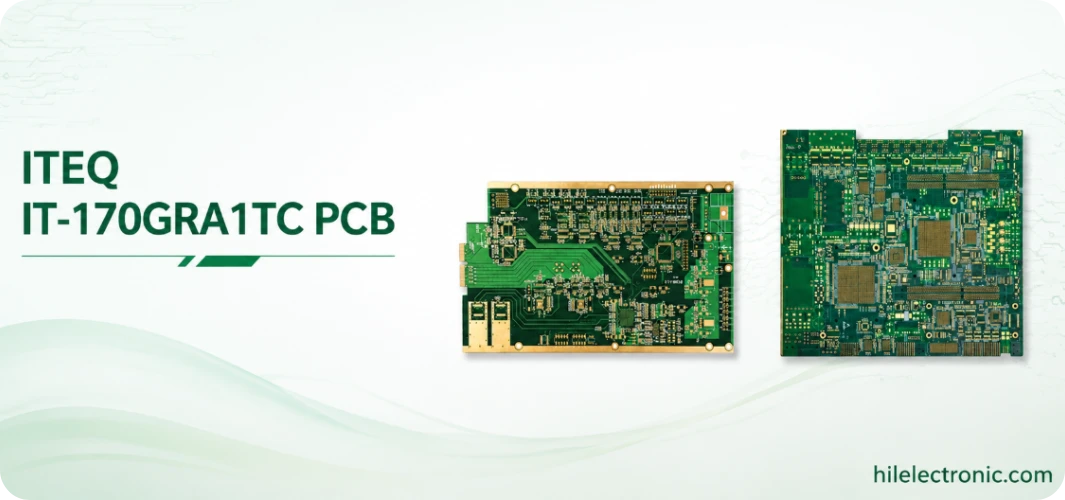
ITEQ IT-170GRA1TC PCB Manufacturer and Material Verification Service
Table of contentsFirst Verify What “IT-170GRA1TC”...
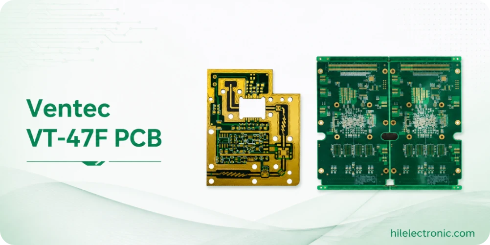
Ventec VT-47F PCB Material Verification Guide: VT-47 or VT-447?
Table of contentsIs VT-47F an Official Ventec PCB...
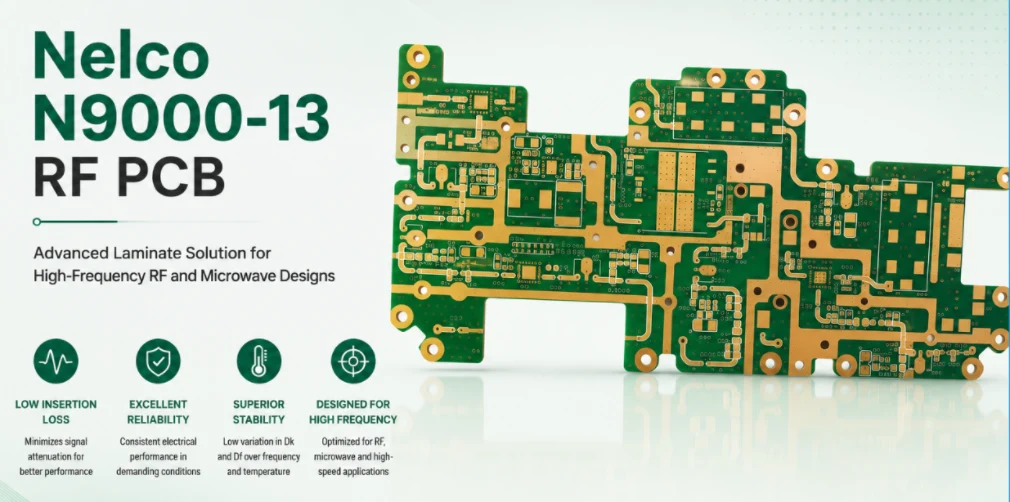
Nelco N9000-13 RF PCB Legacy Manufacturing and Replacement Service
Table of contentsCan Highleap Still Build a Nelco N9000-13...
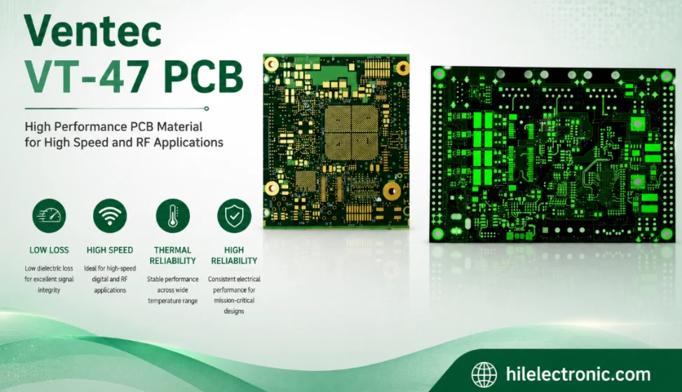
Ventec VT-47 PCB Manufacturer for Reliable High-Tg FR-4 Multilayers
Table of contentsIs Ventec VT-47 the Right High-Tg FR-4...
How to get a quote for PCBs
Let‘s run DFM/DFA analysis for you and get back to you with a report. You can upload your files securely through our website. We require the following information in order to give you a quote:
-
- Gerber, ODB++, or .pcb, spec.
- BOM list if you require assembly
- Quantity
- Turn time
In addition to PCB manufacturing, we offer a comprehensive range of electronic services, including PCB design, PCBA, and turnkey solutions. Whether you need help with prototyping, design verification, component sourcing, or mass production, we provide end-to-end support to ensure your project’s success.
For PCBA services, please provide your BOM (Bill of Materials) and any specific assembly instructions. We also offer DFM/DFA analysis to optimize your designs for manufacturability and assembly, ensuring a smooth production process.