
SMD LED PCB: Technical Guide for Design & Manufacturing

Introduction
SMD LED PCB technology dominates modern lighting, display, and backlighting applications due to its compatibility with automated surface-mount assembly processes. The global LED market continues expanding, with SMD packages accounting for over 70% of LED component shipments across consumer electronics, automotive lighting, and industrial sectors.
However, achieving optimal performance in SMD LED PCB designs requires careful consideration of thermal management, material selection, and manufacturing parameters. This guide addresses the technical complexities engineers face when designing and sourcing SMD LED PCB assemblies, providing actionable specifications and design rules for reliable production.
What is SMD LED
SMD LEDs (Surface-Mount Device Light-Emitting Diodes) are semiconductor light sources designed for direct placement on PCBs using SMT reflow. Unlike through-hole LEDs, they support automated assembly and occupy minimal space. They generate light through electroluminescence, where current passing through a semiconductor junction produces photons at wavelengths defined by the chip materials.
Fundamental Structure
An SMD LED consists of four main parts: the semiconductor die, a metallic lead frame for electrical contact, gold wire bonds linking the die to terminals, and an encapsulation resin (epoxy or silicone) that protects the assembly and shapes light output. This design enables direct soldering to PCB pads without extra hardware.
SMD LED PCB System & Applications
An SMD LED PCB combines the LED with a suitable substrate—FR-4 for low-power use, aluminum-based MCPCB for heat dissipation, or ceramic for high reliability. Supporting circuits include current control, driver ICs, and thermal management to maintain safe junction temperatures. SMD LEDs are widely used in LCD backlighting, architectural and residential lighting strips, electronic status indicators, video walls and signage, automotive lighting, and compact illumination for wearable devices.

SMD LED PCB Packages
Common SMD LED Packages and Key Specifications
Understanding package dimensions and electrical characteristics is fundamental to proper component selection for SMD LED PCB applications. The table below summarizes widely adopted SMD LED packages with their typical operating parameters:
Package
Dimensions (mm)
Typical If (mA)
Typical Output
Primary Applications
Package
Dimensions (mm)
Typical If (mA)
Typical Output
Primary Applications
Package
Dimensions (mm)
Typical If (mA)
Typical Output
Primary Applications
Package
Dimensions (mm)
Typical If (mA)
Typical Output
Primary Applications
Package
Dimensions (mm)
Typical If (mA)
Typical Output
Primary Applications
Package
Dimensions (mm)
Typical If (mA)
Typical Output
Primary Applications
Critical Specifications for SMD LED PCB Design
When selecting components for SMD LED PCB assemblies, engineers must evaluate multiple parameters that directly impact performance and reliability:
- Luminous intensity and flux – Measured in cd or lm, these define brightness and influence optical and thermal design. Higher output requires stronger heat dissipation.
- Correlated Color Temperature (CCT) – Defined in Kelvin and chromaticity coordinates, ranging from warm (2700–3000K) to cool (5000–6500K). Color-critical uses need tight binning, typically within 3-step MacAdam ellipses.
- Color Rendering Index (CRI) – Indicates color accuracy compared to sunlight. General lighting targets CRI ≥80, while retail and medical applications require CRI ≥90.
- Forward voltage and current – Vf is typically 2.8–3.4V at rated current. Power dissipation (P = Vf × If) directly impacts thermal design.
- Beam angle – Ranges from narrow (15–30°) to wide (120–140°), affecting light distribution and optical efficiency.
- Thermal and operating limits – Junction temperature and ambient range define thermal requirements. Keeping Tj 20–30°C below max ratings supports L70 lifetime.
- Reliability parameters – ESD rating, thermal cycling resistance, moisture sensitivity (MSL), and life test data guide manufacturing and durability expectations.
A proper balance of these specifications ensures efficiency, safety, and long-term stability in SMD LED PCB designs. Evaluating them together enables engineers to match LEDs to specific application requirements with confidence.
Recommended Land Patterns for SMD LED PCB
Proper PCB footprint design ensures reliable solder joint formation and optimal heat transfer. For 2835 packages, recommended pad dimensions are 1.6mm × 2.4mm with 0.8mm spacing, using 100% solder paste coverage for optimal wetting. Larger packages like 5050 require 2.2mm × 3.0mm pads with thermal relief vias positioned adjacent to pads when using aluminum substrates.
Solder paste stencil thickness typically ranges from 0.12-0.15mm depending on package size and reflow profile requirements. Thermal via arrays should extend 2-3mm beyond package outlines to capture heat spreading through copper planes on the SMD LED PCB.
SMD LED PCB vs COB LED PCB: Technology Comparison
Chip-on-Board (COB) technology presents an alternative approach where multiple LED dies mount directly onto substrates without individual packaging. Understanding when to select SMD LED PCB versus COB requires evaluating performance trade-offs:
Criteria
SMD LED PCB
COB LED PCB
Criteria
SMD LED PCB
COB LED PCB
Criteria
SMD LED PCB
COB LED PCB
Criteria
SMD LED PCB
COB LED PCB
Criteria
SMD LED PCB
COB LED PCB
Criteria
SMD LED PCB
COB LED PCB
Selection Guidelines
-
COB for uniform illumination – Ideal for applications requiring smooth, shadow-free lighting such as architectural floodlights, high-bay fixtures, and panel lights. The dense die array improves thermal transfer and removes visible point-source artifacts.
-
SMD for scalability and control – Best for projects needing fast assembly, easy maintenance, or color control. Surface-mount production fits existing SMT lines, and RGB or addressable systems rely on SMD PCBs for independent channel management.
-
Thermal considerations – Medium to high-power designs can use aluminum-based SMD PCBs with thermal vias to approach COB performance while retaining flexibility. When power density exceeds ~3 W/cm² or active cooling is required, COB becomes the preferred option.
Types of SMD LED PCB: Material and Configuration Options
Substrate Material Classification
- FR-4 SMD LED PCB – Epoxy-glass laminate used for low-power LEDs under 0.5W. Suitable for indicators, backlighting, and decorative lighting with junction temperatures below 80°C. Multi-layer options allow circuit complexity but offer limited heat dissipation.
- Metal Core PCB (MCPCB) – Aluminum substrates (1.0–2.0 mm) provide better heat spreading for 0.5–5W LEDs. A thermal interface layer with 1–3 W/mK conductivity helps transfer heat from the copper circuit to the metal base.
- Ceramic Substrate PCB – Alumina and aluminum nitride offer high thermal conductivity (20–170 W/mK) and CTE compatibility with LED chips. Ideal for automotive, aerospace, and industrial uses requiring -55°C to +150°C operation and high reliability.
Functional Circuit Categories
- Single-color SMD LED PCBs – Used in general lighting and basic signage. LEDs are wired in simple series or parallel circuits with resistors or linear regulators. Switching converters may be added for better efficiency and heat control.
- RGB / RGBW Modules – Each color channel uses its own driver in common-anode or common-cathode layouts. Accurate current control and microcontroller calibration ensure proper color mixing and compensate for efficiency shifts and aging. PCB layouts separate analog drivers from digital signals to reduce noise.
- Matrix and Display Systems – Include row/column scanning, shift registers, or driver ICs on the PCB. These designs control large LED arrays with fewer connections. Key factors include trace resistance, brightness uniformity, and EMI management.
Density and Application-Specific Designs
- Point-source Designs – Use single LEDs or small clusters for indicators, accent lighting, and signage. PCB layouts prioritize precise LED placement and circuit isolation. Single-sided boards are common for cost and simplicity.
- Linear LED Strips – Typically 30–120 LEDs per meter using 2835, 3528, or 5050 packages. Flexible PCBs suit curved installs, while rigid boards offer better heat dissipation. Designs account for voltage drop with wider traces and added power injection points.
- Area Light Panels – LEDs are distributed across flat or custom shapes for backlighting, task lighting, or architectural use. Higher power density demands strong thermal management with vias or active cooling. Diffusers or light guides ensure uniform illumination.
Manufacturing Process Considerations
- SMT Reflow Assembly – Most SMD LED PCBs use lead-free reflow with peak temperatures of 240–250°C for 20–40 seconds. Nitrogen reflow reduces oxidation and improves solder joints, especially on aluminum boards where heating must be controlled.
- Protective and Secondary Processes – Potting, conformal coating, and lens attachment add moisture and environmental protection. UV adhesives secure optics, while selective coating avoids blocking heat paths. IP65–IP68 designs use gaskets and filled thermal vias for full sealing.

SMD LED PCB
SMD LED PCB Design and Manufacturing Best Practices
Thermal Management for SMD LED PCB
Efficient thermal paths must transfer heat from the LED die to the ambient environment through the package, solder joint, copper pad, vias, and heatsink.
- Copper thickness – Using 2–3 oz (70–105 μm) copper reduces thermal resistance versus standard 1 oz. Wider traces improve heat spreading.
- Thermal vias – Vias of 0.3–0.4 mm diameter with 0.6–1.0 mm spacing balance performance and manufacturability. Arrays placed at the thermal pad serve as the main conduction route. Filled vias eliminate air gaps.
Electrical Design for SMD LED PCB
Constant current drivers ensure reliable operation and consistent brightness, unlike resistor-based limiting.
- LED string design – Series strings lower current but need higher voltage. Parallel strings support lower voltages but require current balancing. Mixed configurations optimize power distribution.
- PWM dimming – Frequencies above 200–300 Hz prevent flicker. Low-ESR capacitors near outputs reduce noise, and separate ground planes limit interference with control signals.
Assembly Process for SMD LED PCB
- Solder paste – SAC305 suits most uses; SAC405 improves performance on aluminum boards in higher temperatures.
- Reflow profile – Aluminum substrates need tailored profiles. Typical cycles use a 60–90 s preheat to 150–180°C and 240–245°C peak with 20–30 s above liquidus.
- Placement accuracy – Pick-and-place systems typically achieve ±0.05 mm. Optical-critical designs may need vision guidance or post-reflow adjustment.
Design for Manufacturing Verification
A complete documentation package includes:
- BOM with LED package, voltage, brightness, and color bins
- Fabrication data with copper weight, finish (ENIG or OSP), and via details
- Assembly requirements: solder paste, reflow profile, and optical alignment
- Thermal testing points and criteria
- Reliability plan covering HTOL, thermal cycling, and humidity tests
Choosing the right partner is key to performance and long-term reliability. Contact us to develop SMD LED PCB solutions that meet your exact technical and production requirements.
Reliability Testing for SMD LED PCB
To ensure long-term performance and durability, SMD LED PCBs undergo a series of reliability tests designed to simulate real operating environments and stress conditions:
-
Thermal shock cycling – -40°C to +85°C/+105°C for 500–1000 cycles to validate solder joint reliability and material stability.
-
Temperature-humidity-bias (THB) – 85°C/85% RH with electrical bias to identify moisture sensitivity and electrochemical failure risks.
-
Operating lifetime testing – Run at rated conditions to measure lumen maintenance and determine L70 performance.
-
Electrostatic discharge (ESD) testing – Conducted per ANSI/ESDA/JEDEC JS-001 to confirm resistance to handling damage.
-
Mechanical testing – Vibration and shock per IEC standards for automotive, industrial, and transportation uses.
-
Solder joint inspection – Microsection analysis verifies attachment quality and fillet formation.
These testing protocols help manufacturers confirm that SMD LED PCB assemblies meet application requirements and maintain performance over their intended service life.
Conclusion
SMD LED PCB technology enables high-performance lighting and display solutions through proper component selection, thermal control, and manufacturing. Success depends on balancing optical output, thermal limits, electrical design, and cost. Engineers must define binning requirements, validate thermal performance through testing, and work with reliable suppliers to ensure quality and consistency.
Highleap Electronics SMD LED PCB Capabilities
Highleap Electronics provides comprehensive SMD LED PCB solutions from prototype through volume production:
- Engineering support – Thermal design optimization, component selection guidance, and DFM review ensuring manufacturability at scale for SMD LED PCB projects.
- Advanced manufacturing – In-house aluminum substrate fabrication, high-precision SMT assembly with optical inspection, and environmental testing validating performance across operating conditions.
- Component sourcing – Relationships with leading LED suppliers enabling access to latest package technologies and competitive binning options for SMD LED PCB assemblies.
- Quality certifications – ISO 9001 and ISO 13485 certified quality management systems with full traceability and reliability documentation supporting automotive, medical, and industrial applications.
- Application expertise – Proven experience across simple indicator assemblies, complex RGB matrix displays, and high-power architectural lighting using SMD LED PCB technology.
Ready to improve performance and manufacturability? Contact Highleap Electronics for engineering support and a competitive quote. Our team guides you from concept to production, helping you meet targets on time and within budget.

Recommended Posts

RF Transceiver PCB Manufacturing and Assembly
Table of contentsRF Transceiver PCB Manufacturing and...
RFSoC Board PCB Manufacturing and Assembly One-Stop Service
Highleap Electronics supports customer-designed RFSOC...
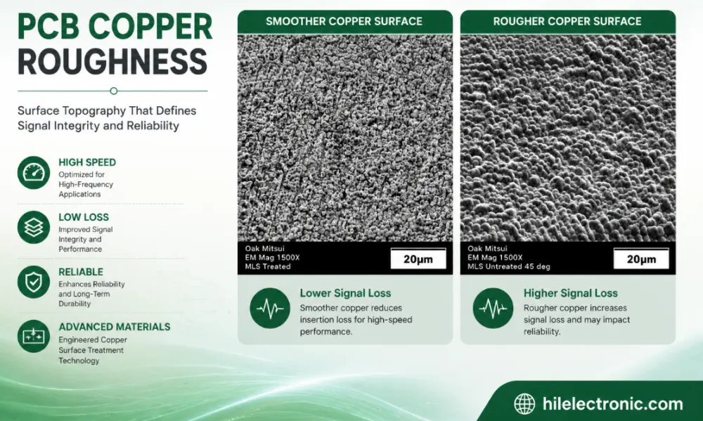
PCB Copper Roughness: Signal Loss, Material Selection and Manufacturing Control
Table of contentsWhat Is PCB Copper Roughness?How Copper...
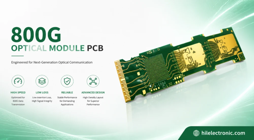
800G Optical Module PCB Manufacturing and Assembly Service
Table of contentsWhat Makes an 800G Optical Module PCB...
How to get a quote for PCBs
Let‘s run DFM/DFA analysis for you and get back to you with a report. You can upload your files securely through our website. We require the following information in order to give you a quote:
-
- Gerber, ODB++, or .pcb, spec.
- BOM list if you require assembly
- Quantity
- Turn time
In addition to PCB manufacturing, we offer a comprehensive range of electronic services, including PCB design, PCBA, and turnkey solutions. Whether you need help with prototyping, design verification, component sourcing, or mass production, we provide end-to-end support to ensure your project’s success.
For PCBA services, please provide your BOM (Bill of Materials) and any specific assembly instructions. We also offer DFM/DFA analysis to optimize your designs for manufacturability and assembly, ensuring a smooth production process.