
The PCB Layout Design Process

Designing a PCB is a meticulous process that begins with conceptualizing and ultimately results in a physical board ready for manufacturing. Central to this design process is the transformation of an initial schematic diagram into an actionable PCB layout, accomplished using Computer-Aided Design (CAD) tools. This guide will break down the various stages involved in PCB layout design, highlighting essential steps for creating efficient, high-quality PCBs.
Overview of the PCB Layout Design Process
Becoming a proficient PCB designer requires understanding each step of the layout design process. A well-planned design ensures the final product functions as intended, while minimizing errors and production delays. Below, we’ll walk through the various stages involved in PCB layout design, from conceptualization to manufacturing.
Step 1: Creating the Schematic Diagram
The design journey begins with drawing a schematic diagram, which serves as a logical representation of the circuit’s components and their connections. Each component is represented by standard symbols, with electrical connections (or nets) drawn between them. These nets will eventually translate into copper traces on the final PCB.
The schematic is typically created using PCB design software like Altium Designer, Eagle, or OrCAD. In this stage, the designer arranges the symbols of various components (resistors, capacitors, ICs, etc.) and ensures all electrical connections are logically sound.
-
Schematic Symbol Creation: Each component is defined by a symbol, which must include pins for electrical connections. These symbols must align with the physical components that will be used in the final design.
-
Netlist Generation: Once the schematic is complete, a netlist is generated. This list defines all electrical connections between components and will be used in the PCB layout phase to route the electrical signals.
Step 2: Pre-Layout Preparations
Once the schematic is validated, the pre-layout stage begins. This stage involves setting up essential parameters and verifying that all necessary components are available for manufacturing.
-
BOM (Bill of Materials) Validation: The BOM is a crucial document that lists all the components required for the PCB. During validation, designers ensure that all parts are current, correctly specified, and not obsolete. Manufacturer part numbers (MPNs) are checked for accuracy, and any obsolete or unavailable components are identified.
-
Stack-up Design: The stack-up defines how layers of the PCB are arranged. Designers need to determine the number of signal layers, power layers, and ground layers based on the project’s requirements. This step often requires coordination with the manufacturer to select the right materials (e.g., FR4, Rogers) and ensure proper impedance control.
Step 3: PCB Layout
With the schematic and pre-layout checks in place, the PCB layout stage begins. This is where the actual design of the PCB takes shape.
-
Setting Board Parameters: The first step in layout is defining the board outline and establishing design rules. The stack-up and layer configuration are specified here, and all constraints related to trace widths, via sizes, and clearances are set.
-
Component Placement: Effective component placement is crucial for a functional PCB. Designers group components based on their function (e.g., analog, digital, power) and place them in a manner that minimizes signal interference and optimizes routing. Critical components like connectors and ICs are placed first, followed by auxiliary components.
-
Routing: Routing the copper traces between components is one of the most vital tasks in PCB layout. Interactive routing tools allow the designer to create traces that connect pins in the schematic. The traces are placed on copper layers, and vias are used to connect different layers.
-
Power and Ground Planes: Power and ground connections are essential for reducing noise and ensuring stable operation. Designers typically dedicate an entire layer to the ground plane and another to the power plane to maintain proper signal integrity.
-
Design Rule Check (DRC): A Design Rule Check (DRC) ensures that the PCB layout adheres to all design constraints. This includes checking trace widths, spacing, and via sizes. DRC is performed throughout the design process to catch any potential issues before they become problems.
Step 4: Generating Production Files
Once the PCB layout is complete and all design checks are satisfied, the next step is to generate production files. These files will be used by the manufacturer to fabricate the PCB.
-
Gerber Files: The primary output of the PCB design process is the Gerber files. These files define the copper layers, solder mask layers, silkscreen layers, and drill holes. Each layer is represented in a specific file format, including the top and bottom copper layers, solder mask, silkscreen, and more.
-
Drill Files: A drill file specifies the location, size, and type of holes required for component leads and vias.
-
Assembly Drawings: These drawings provide additional information about the assembly process, such as component placement, part numbers, and orientation.
Step 5: Design for Manufacturability (DFM) and Final Checks
Before the PCB is sent to production, a final Design for Manufacturability (DFM) check is essential. DFM analysis reviews the layout for any manufacturing issues, such as trace widths that are too small or improperly placed components. DFM checks ensure that the PCB can be reliably fabricated and assembled without costly rework or delays.
At this stage, designers also ensure that DFM guidelines are followed to minimize risks during fabrication. This can involve checking for common manufacturing issues, such as via breakout problems, trace spacing violations, or incorrect drill sizes.
Tools and Software for PCB Layout Design
To efficiently design a PCB, engineers typically use Electronic Design Automation (EDA) tools. These tools provide advanced features for schematic capture, layout design, and design validation.
-
Altium Designer: A comprehensive tool for PCB layout and design, providing integrated schematic capture, routing, and advanced simulation capabilities.
-
Eagle: A widely-used, user-friendly PCB design tool with a robust set of features suitable for small to medium-sized designs.
-
OrCAD: Known for its powerful simulation and PCB layout features, OrCAD is used in more complex designs.
Conclusion
The PCB layout design process is complex and requires careful attention to detail at every step. From schematic creation to pre-layout validation, component placement, routing, and finally, generation of production files, each stage plays a vital role in creating a functional, manufacturable PCB. By following established design procedures and utilizing powerful PCB design tools, engineers can ensure that the final product meets all performance, cost, and manufacturability requirements.
By incorporating proper checks and validation throughout the design process, PCB designers can optimize for reliability, manufacturability, and efficiency, ensuring a successful and smooth transition from design to production.
FAQs
How can PCB layout be optimized to improve signal integrity?
Signal integrity is critical for ensuring the reliable and efficient operation of a circuit. Optimizing signal integrity can be achieved through several strategies, such as carefully choosing signal paths, avoiding long traces and cross-talk interference, using appropriate termination resistors for high-frequency signals, ensuring continuity in the power and ground planes, and using differential pairs when necessary. These design techniques can reduce signal reflection, noise interference, and crosstalk, ultimately enhancing the stability and performance of the circuit.
How do you select the appropriate materials for PCB design?
The choice of PCB materials directly impacts the performance and manufacturing costs of the board. Common PCB materials include FR4, Rogers, and Polyimide, among others. When selecting materials, factors such as the operating frequency, thermal management requirements, dielectric constant, temperature tolerance, and expected production volume must be considered. For instance, Rogers materials are preferred for high-frequency applications due to their low dielectric constant and thermal stability, while FR4 is commonly used for general low-frequency circuits. Designers need to balance application-specific needs, cost constraints, and manufacturer recommendations when selecting materials.
How can electromagnetic interference (EMI) be minimized or avoided in PCB design?
Electromagnetic interference (EMI) is a common challenge, especially in high-frequency or high-power circuits. Strategies to minimize EMI include properly arranging power and ground planes to reduce noise, using appropriate decoupling capacitors and filters, optimizing PCB layer stacking and trace width, using shielding (metal enclosures or grounded planes), and implementing differential signal routing. Additionally, keeping sensitive signal lines away from power or ground layers, and maintaining proper trace spacing, can help mitigate EMI and improve circuit performance.
How can heat dissipation be effectively managed for high-power components in PCB design?
High-power components, such as power amplifiers, transformers, and high-power LEDs, generate significant heat during operation and require effective thermal management in the PCB design. Common thermal management techniques include using heat sinks or heat pipes, designing thicker copper layers to conduct heat more efficiently, placing high-power components in areas with good airflow or heat dissipation, and ensuring proper layer stacking for thermal conductivity. Additionally, using thermal vias and optimizing component layout to distribute heat evenly can prevent localized overheating and improve the long-term reliability of the PCB.
How can PCB design reliability be improved, particularly for high-temperature and high-humidity environments? To enhance PCB reliability in harsh environments, such as high temperature and high humidity, several design measures should be taken. These include selecting materials that are resistant to high temperatures and moisture (e.g., high-temperature-rated FR4 or ceramic substrates), optimizing soldering processes to ensure strong and reliable joints, designing proper heat dissipation for components, ensuring moisture protection through sealed enclosures or coatings, and incorporating corrosion-resistant materials. These strategies help ensure the PCB’s longevity and reliability in challenging operating conditions.
Get a Free PCB & PCBA Quote

Recommended Posts
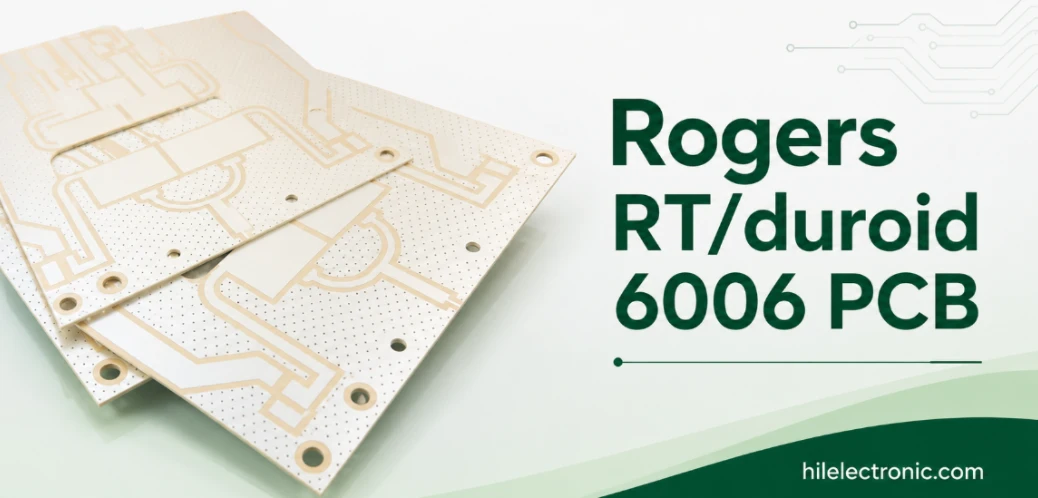
RT/duroid 6006 PCB Manufacturer for Compact High-Dk Microwave Circuits
RT/duroid 6006 is selected when circuit area is expensive....
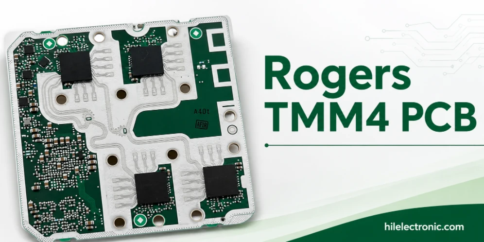
Rogers TMM4 PCB Manufacturer for Compact Microwave Filters
TMM4 is most useful when a microwave circuit must become...
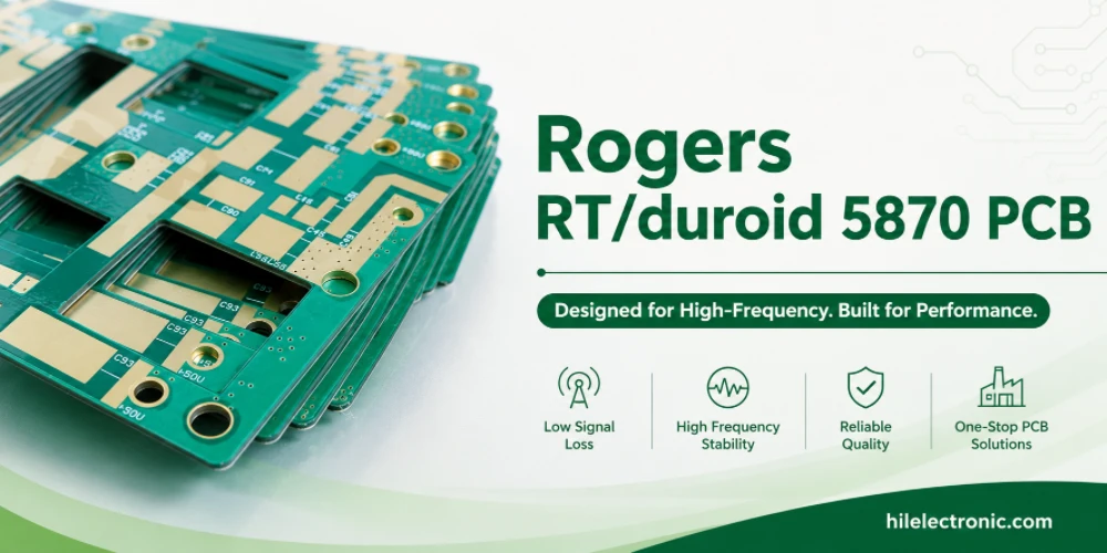
RT/duroid 5870 PCB Manufacturer for Low-Loss PTFE RF Circuits
RT/duroid 5870 is chosen when the RF path needs low loss,...
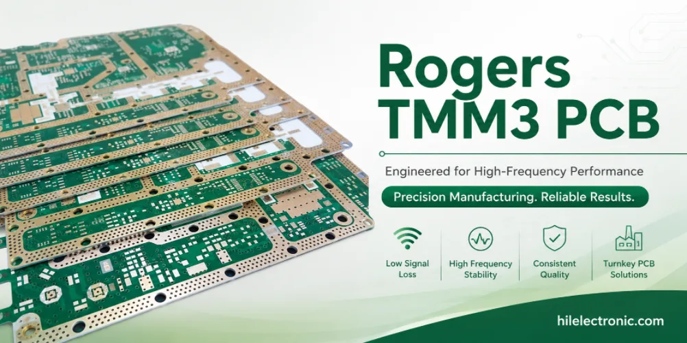
Rogers TMM3 PCB Manufacturer for Mechanical RF Modules
TMM3 is selected when an RF circuit must behave as part of...
How to get a quote for PCBs
Let us run DFM/DFA analysis for you and get back to you with a report.
You can upload your files securely through our website.
We require the following information in order to give you a quote:
-
- Gerber, ODB++, or .pcb, spec.
- BOM list if you require assembly
- Quantity
- Turn time
In addition to PCB manufacturing, we offer a comprehensive range of electronic services, including PCB design, PCBA (Printed Circuit Board Assembly), and turnkey solutions. Whether you need help with prototyping, design verification, component sourcing, or mass production, we provide end-to-end support to ensure your project’s success. For PCBA services, please provide your BOM (Bill of Materials) and any specific assembly instructions. We also offer DFM/DFA analysis to optimize your designs for manufacturability and assembly, ensuring a smooth production process.