
Medical Device Ceramic PCB: Precision Substrates for Advanced Medical Electronics

Introduction
Modern medical electronics demand exceptional electrical insulation, precise thermal management, and proven material safety to ensure patient wellbeing and device longevity. Medical device ceramic PCBs have emerged as the substrate of choice for applications where conventional circuit boards fall short. Unlike organic materials, ceramic substrates offer superior thermal conductivity, zero outgassing, and inherent biocompatibility that meet stringent regulatory requirements.
This article examines the key performance attributes, typical applications, and design considerations that make ceramic substrates the preferred solution for precision medical electronics.
Why Medical Device Ceramic PCBs Are Ideal for Medical Electronics
Limitations of Conventional PCB Materials
FR-4 and metal-core PCBs fall short in medical environments that demand extreme reliability and cleanliness. FR-4 contains organic resins that degrade under heat or release volatile compounds, while metal-core substrates, though thermally efficient, lack the electrical insulation required for high-voltage medical circuits.
Advantages of Inorganic Ceramic Substrates
Ceramic PCBs eliminate these drawbacks through their fully inorganic composition. Free from resins or binders, they prevent contamination and maintain exceptional purity. With dielectric loss tangents below 0.001 across wide frequency ranges, alumina and aluminum nitride ceramics ensure signal integrity in sensitive diagnostic and sensing applications.
Thermal, Chemical, and Dimensional Stability
Ceramic substrates remain stable from cryogenic temperatures to above 300 °C without warping or performance drift. Their near-zero moisture absorption prevents swelling and electrical variation during autoclave sterilization. This combination of thermal endurance, chemical inertness, and dimensional stability makes ceramic PCBs ideal for long-life implantable and sterilizable medical devices.
Key Performance Benefits of Medical Device Ceramic PCBs
High Precision Circuit Performance
Medical device ceramic PCB substrates support trace widths and spacing below 50 micrometers, enabling the dense circuit layouts required for miniaturized sensor modules and multi-channel imaging arrays. The near-zero coefficient of thermal expansion mismatch with silicon semiconductors prevents solder joint fatigue in flip-chip assemblies. Surface roughness values under 0.2 micrometers minimize signal loss in high-frequency RF circuits used for wireless telemetry and diagnostic imaging.
Thermal Stability and Heat Dissipation
Aluminum nitride ceramic substrates achieve thermal conductivity values exceeding 170 W/mK, approaching that of pure copper while maintaining electrical insulation. This thermal performance proves critical in laser driver circuits and LED surgical lighting where concentrated heat generation would cause measurement drift or component failure on conventional substrates. The uniform heat spreading capability of medical device ceramic PCB assemblies eliminates hot spots that accelerate aging in precision analog circuits.
Biocompatibility and Safety
Alumina and aluminum nitride ceramics satisfy ISO 10993 biocompatibility testing requirements for both short-term tissue contact and long-term implantation. The chemical stability of these materials prevents ion leaching that could trigger inflammatory responses or interfere with cellular function. Medical device ceramic PCB substrates maintain their inert properties through decades of exposure to body fluids, making them suitable for pacemakers and neurostimulators where device replacement surgeries must be minimized.
Chemical and Radiation Resistance
Ceramic substrates withstand repeated exposure to hydrogen peroxide plasma, ethylene oxide, and gamma radiation sterilization without surface degradation or electrical property changes. This durability extends to harsh chemical environments in diagnostic analyzers where reagents might attack organic circuit board materials. The radiation hardness of medical device ceramic PCB assemblies proves essential in X-ray detection arrays and CT scanner electronics positioned in high-flux radiation fields.
Longevity and Reliability
Medical devices often require operational lifetimes exceeding fifteen years with failure rates below one per million device-hours. Ceramic substrates lack the organic degradation mechanisms that limit FR-4 board lifetimes, including delamination, conductive anodic filament growth, and intermetallic compound formation at elevated temperatures. Accelerated life testing demonstrates that properly designed medical device ceramic PCB assemblies maintain stable electrical parameters through thermal cycling and humidity exposure equivalent to decades of implanted service.

Typical Applications of Medical Device Ceramic PCBs
Medical device ceramic PCB technology serves critical functions across multiple categories of medical equipment, each with distinct performance requirements and reliability expectations. The following applications demonstrate how ceramic substrates enable advanced medical electronics.
| Application Category | Example Devices | Key Requirements |
|---|---|---|
| Implantable Devices | Pacemakers, cochlear implants, neurostimulators | Long-term biocompatibility, hermetic reliability, zero outgassing |
| Diagnostic Systems | X-ray detectors, ultrasound transducers, MRI coils | High thermal dissipation, radiation resistance, signal integrity |
| Therapeutic Equipment | Laser drivers, electrosurgical units, RF ablation systems | High voltage isolation, power handling, thermal management |
| Monitoring Devices | Patient sensors, temperature transducers, pressure monitors | Miniaturization, sterilization resistance, calibration stability |
Implantable Devices
Cardiac pacemakers utilize alumina ceramic substrates to house battery management circuits and RF telemetry modules in hermetically sealed titanium cases. Cochlear implants mount electrode stimulation drivers on ceramic carriers that provide both electrical isolation and thermal dissipation for the signal processing circuitry. Neurostimulators for pain management and Parkinson’s disease treatment rely on medical device ceramic PCB technology to deliver calibrated electrical pulses without drift over the device lifetime.
Diagnostic Systems
X-ray detector arrays bond scintillator crystals and photodiode arrays to aluminum nitride substrates that efficiently conduct heat away from the active detection area while providing electrical isolation between thousands of individual pixel channels. Ultrasound transducer assemblies use ceramic substrates to support piezoelectric element arrays and integrated preamplifiers in configurations that would overheat on conventional circuit boards. MRI gradient coil drivers generate kilowatts of pulsed power in confined spaces where medical device ceramic PCB thermal management prevents component damage and maintains imaging precision.
Therapeutic Equipment
Surgical laser systems mount high-power diode bars and driver circuits on ceramic substrates that spread thermal loads across larger areas than metal-core boards can achieve while maintaining electrical isolation. Electrosurgical generators use ceramic substrates in their RF power stages where voltage isolation requirements exceed the capabilities of laminate materials.
Monitoring Devices
Patient monitoring sensors for temperature, pressure, and blood oxygen saturation integrate signal conditioning circuits on miniature ceramic substrates that fit within catheter-mounted assemblies. The stable dielectric properties of medical device ceramic PCB materials ensure that sensor calibration remains accurate through repeated sterilization cycles and years of clinical use.
Material Selection for Medical Device Ceramic PCBs
The choice of ceramic material directly impacts the electrical performance, thermal management capability, and cost structure of medical device ceramic PCB assemblies. Each material offers distinct advantages for specific application requirements.
| Ceramic Material | Thermal Conductivity | Dielectric Constant | Typical Medical Applications |
|---|---|---|---|
| Alumina (Al₂O₃) 96% | 20-24 W/mK | 9.0-10.0 | General medical devices, signal processing, low-power circuits |
| Alumina (Al₂O₃) 99.6% | 28-35 W/mK | 9.8-10.2 | High-reliability implantables, precision sensors, RF circuits |
| Aluminum Nitride (AlN) | 170-200 W/mK | 8.6-8.9 | High-power LED arrays, laser drivers, MRI electronics |
| Silicon Nitride (Si₃N₄) | 15-30 W/mK | 7.0-8.0 | High-frequency power modules, imaging detectors, thermal shock environments |
Alumina (Al₂O₃)
Alumina ceramic substrates offer dielectric strength exceeding 15 kV/mm and volume resistivity above 10¹⁴ ohm-cm at room temperature, making them suitable for high-voltage isolation in diagnostic imaging equipment and therapeutic devices. With a cost structure significantly lower than aluminum nitride, alumina serves as the workhorse material for general medical electronics. Medical device ceramic PCB assemblies using 96 percent or 99.6 percent purity alumina provide the electrical performance and mechanical strength needed for most applications while maintaining economical production costs.
Aluminum Nitride (AlN)
Applications requiring thermal conductivity above 150 W/mK specify aluminum nitride substrates despite their higher material cost. The combination of excellent heat spreading and low dielectric constant makes aluminum nitride the preferred choice for RF power amplifiers in MRI systems and high-brightness LED arrays in surgical lighting. Medical device ceramic PCB designs using aluminum nitride can operate at higher power densities than alumina-based assemblies, enabling more compact device architectures where space constraints are critical.
Silicon Nitride (Si₃N₄)
Silicon nitride substrates excel in applications demanding superior mechanical strength and resistance to thermal shock. The material’s fracture toughness exceeds that of alumina by a factor of three, reducing the risk of substrate cracking during assembly operations or device deployment. While less common than alumina or aluminum nitride in medical device ceramic PCB applications, silicon nitride offers unique advantages for specialized high-reliability requirements in high-frequency power modules and imaging detector arrays.
Design Considerations for Medical Device Ceramic PCBs
Circuit Layout and Thermal Management
Circuit layout for medical device ceramic PCB assemblies must account for the brittleness of the base material through careful placement of mounting holes and edge clearances. Thermal management design requires explicit modeling of heat flow paths since the high thermal conductivity of the substrate creates different temperature distributions than designers familiar with FR-4 boards might expect.
Key design factors include:
- Via structure optimization – Connecting multiple metallization layers requires larger diameters and careful aspect ratio control compared to drilled copper plating in organic boards.
- Thermal path planning – Direct heat flow from high-power components to heat sinks through the ceramic substrate minimizes junction temperatures and extends device lifetime.
- Metallization selection – Thick film processes using screen-printed gold or platinum-silver conductors provide robust adhesion and wire bonding compatibility, while thin film approaches enable finer feature sizes for high-density interconnect.
- Surface finish specification – Coating selection must consider the planned attachment methods, whether solder reflow, conductive adhesive bonding, or wire bonding to semiconductor dies.
Assembly and Packaging Compatibility
Medical device ceramic PCB designs must accommodate standard semiconductor packaging formats including BGA, LGA, and flip-chip configurations while maintaining thermal and electrical performance. The coefficient of thermal expansion match between ceramic substrates and silicon devices enables reliable attachment without underfill materials in many applications. Hermetic sealing requirements for implantable devices demand precise substrate flatness and surface finish control to achieve reliable brazed or welded seals with titanium or stainless steel enclosures.

Manufacturing Standards for Medical Device Ceramic PCBs
Quality Management and Traceability
ISO 13485 certification provides the quality management framework required for medical device component manufacturing. Ceramic substrate fabrication facilities must implement full material traceability from incoming raw materials through finished goods, with documentation demonstrating process control at each manufacturing step. Clean room assembly environments prevent particulate contamination that could create electrical leakage paths or compromise hermetic sealing in implantable devices.
Process Control and Validation
Laser cutting and scribing technologies create precise substrate dimensions and complex edge geometries without introducing the microcracks that mechanical sawing can generate. Automated optical inspection systems verify metallization integrity, dimensional accuracy, and surface cleanliness before substrates enter the assembly process. Medical device ceramic PCB manufacturers employ statistical process control to maintain tight tolerances on critical parameters including dielectric strength, thermal resistance, and metallization adhesion that directly affect device safety and reliability.
Critical manufacturing controls include:
- Incoming material certification – Raw ceramic materials require vendor certification for purity, grain size, and physical properties to ensure consistent substrate performance.
- Metallization process validation – Thick film firing profiles and thin film deposition parameters undergo periodic verification to maintain adhesion strength and electrical conductivity within specification limits.
- Dimensional inspection protocols – Coordinate measuring machines and optical metrology systems document substrate flatness, thickness variation, and feature placement accuracy for full traceability.
- Accelerated life testing – Validation requirements for medical applications extend beyond standard PCB acceptance testing to include biocompatibility verification, aging studies, and failure mode analysis.
These manufacturing controls ensure that every ceramic PCB used in medical devices meets stringent reliability and safety standards. By maintaining tight process validation, dimensional accuracy, and long-term material stability, manufacturers can guarantee consistent electrical performance and biocompatibility across production batches — a critical requirement for life-supporting and diagnostic medical equipment.
Conclusion
Medical device ceramic PCB technology delivers the unique combination of biocompatibility, thermal performance, and long-term reliability that modern medical electronics require. The inorganic nature of ceramic substrates eliminates outgassing and chemical leaching concerns while providing electrical insulation and heat dissipation capabilities unmatched by conventional circuit board materials.
From implantable cardiac devices requiring decades of stable operation to diagnostic imaging systems managing high power densities, ceramic substrates enable medical innovations that improve patient outcomes and device longevity.
Highleap Electronics brings comprehensive capabilities to medical device ceramic PCB manufacturing and assembly:
- ISO 13485-certified production facilities – Full quality management systems ensuring regulatory compliance and complete material traceability for medical device components.
- Advanced ceramic substrate fabrication – Precision laser cutting, thick film and thin film metallization processes, and automated inspection systems maintaining tight tolerances on critical electrical and mechanical parameters.
- Clean room assembly services – Contamination-controlled environments for component placement, wire bonding, and hermetic sealing operations meeting the stringent cleanliness requirements of implantable and diagnostic medical devices.
- Engineering support and design collaboration – Technical expertise in ceramic material selection, thermal management optimization, and design for manufacturability helping medical device developers navigate the transition from prototype to volume production.
Contact Highleap Electronics to discuss how our medical device ceramic PCB manufacturing capabilities can support your next-generation medical electronics project with the precision, reliability, and regulatory compliance that patients and healthcare providers demand.

Recommended Posts
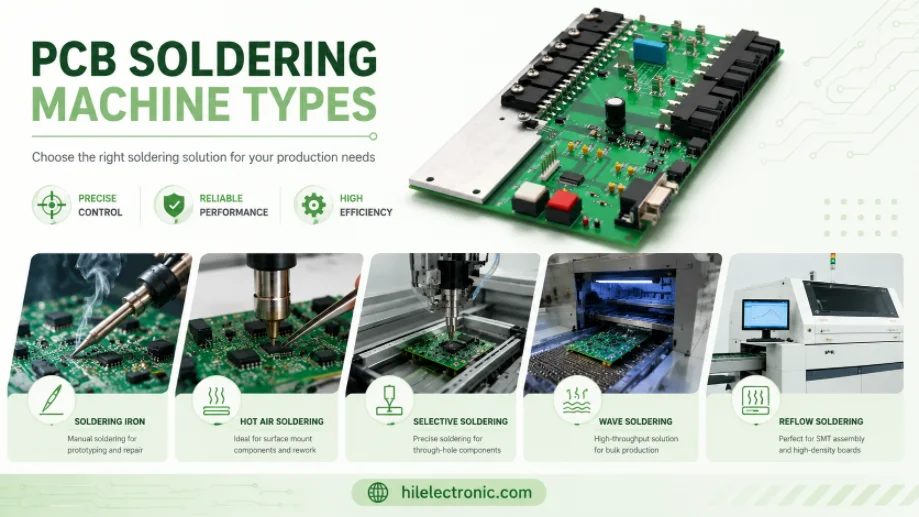
PCB Soldering Machine Types: Reflow, Wave, and Selective Equipment
Figure 1. PCB soldering machine types image for Highleap...
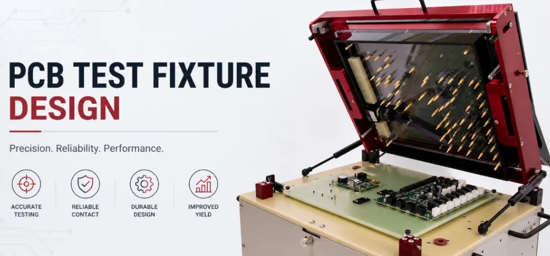
PCB Test Fixture Design: Bed-of-Nails, Flying Probe, and DFT
Figure 1. PCB test fixture design image for Highleap...

Clean Flux vs No-Clean Flux: Residue, Cleaning, and PCB Reliability
Figure 1. clean flux vs no-clean flux image for Highleap...
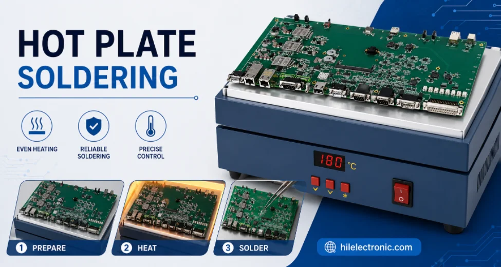
Hot Plate Soldering: Process, Limits, and Reflow Comparison
Figure 1. hot plate soldering image for Highleap...
How to get a quote for PCBs
Let‘s run DFM/DFA analysis for you and get back to you with a report. You can upload your files securely through our website. We require the following information in order to give you a quote:
-
- Gerber, ODB++, or .pcb, spec.
- BOM list if you require assembly
- Quantity
- Turn time
In addition to PCB manufacturing, we offer a comprehensive range of electronic services, including PCB design, PCBA, and turnkey solutions. Whether you need help with prototyping, design verification, component sourcing, or mass production, we provide end-to-end support to ensure your project’s success.
For PCBA services, please provide your BOM (Bill of Materials) and any specific assembly instructions. We also offer DFM/DFA analysis to optimize your designs for manufacturability and assembly, ensuring a smooth production process.