
5 Things You Need To Pay Attention To When Flex PCB Soldering

Soldering flexible printed circuit boards (PCBs) is a delicate process that demands precision and a deep understanding of the materials and conditions involved. Unlike traditional rigid PCBs, flexible PCBs come with unique challenges due to their bendable nature and the materials used in their construction. Whether you are working on flexible circuits for consumer electronics, medical devices, or industrial applications, achieving optimal performance requires an approach tailored to the specific needs of flex PCBs. Here, we provide a comprehensive guide with essential tips for successful soldering, common mistakes to avoid, and advanced solutions to common issues.
Key Tips for Successful Soldering of Flexible PCBs
1. Choosing the Right Substrate for Stability and Durability
The substrate is the backbone of any PCB, offering structural integrity and support. For flex PCBs, the choice of substrate is even more critical, as it must combine flexibility with durability. Materials such as Kapton and polyimide films are commonly used for their flexibility, thermal stability, and resistance to mechanical stress. In high-frequency applications, materials like RO3000 and RO4000 are preferred for their low dielectric loss and flexibility.
Pro Tip: Select a substrate that matches the environmental conditions of the final application, focusing on thermal stability and flexibility based on the operating environment.
2. Managing Heat Carefully
Due to their softer materials, flex PCBs are more susceptible to heat damage compared to rigid boards. Excessive heat during the soldering process can lead to warping, damaging the PCB and components. To avoid this, it’s essential to carefully manage the heat during the soldering process.
One effective method is using thermal interface materials like thermal paste or heat sinks to evenly distribute heat, preventing localized hot spots. Additionally, ensure that your soldering equipment is calibrated to maintain consistent and controlled temperatures.
Pro Tip: Apply heat gradually and avoid sudden temperature spikes to prevent thermal shock and warping.
3. Optimizing Component Layout and Orientation
Proper component layout is essential for effective soldering. Misalignment or incorrect orientation of components can lead to soldering defects that are challenging to fix. Make sure that all components are correctly oriented and aligned in the same direction. Maintain sufficient space between components to facilitate easy soldering and post-soldering inspections. Avoid placing SMD components on both sides of the PCB to prevent heat distribution issues during soldering.
Pro Tip: If adhesive is used to fix components, maintain at least a 3mm gap between components to allow heat to flow evenly during the process.
4. Mastering Solder Paste Printing
Solder paste printing is a crucial aspect of flex PCB assembly. Proper application ensures reliable electrical and mechanical connections. Poor paste application can lead to over-soldering or under-soldering defects, which can compromise the PCB’s performance.
To optimize solder paste printing, use high-quality stencils and ensure that the printer is correctly calibrated. Proper paste application can improve PCB reliability by up to 60%.
Pro Tip: Calibrate your solder paste printer and use accurate stencils to ensure optimal paste distribution and reduce the risk of defects.
5. Addressing Planarity Issues
Maintaining a flat surface during soldering is one of the biggest challenges when working with flex PCBs. Due to their flexible nature, these boards are prone to bowing and twisting, which can affect the quality of solder joints. To mitigate these issues, consider using RoHS-compliant and pre-preg materials to prevent warping. Avoid rapid temperature changes during soldering to reduce the risk of flexing and thermal shock.
Pro Tip: Use a steady and gradual temperature profile during soldering to minimize flexing and thermal shock, ensuring the board remains flat.
Common Mistakes to Avoid in Flex PCB Soldering
Even experienced professionals can fall prey to common soldering mistakes. Here are some pitfalls to watch out for:
Mistake 1: Choosing the Wrong PI Substrate
Selecting an unsuitable substrate can lead to warping after multiple reflow cycles. For instance, using a standard PI substrate with a Coefficient of Thermal Expansion (CTE) of 35ppm/°C can result in significant warping, while a modified PI substrate with a CTE of 18ppm/°C will provide much better results.
Solution: Opt for substrates with a temperature tolerance ≥280°C and a peel strength >1.2N/mm.
Mistake 2: Incorrect Temperature Profile Settings
Excessive heating rates during soldering can cause delamination of the cover film. It’s important to use a dynamic RTS (Ramp-to-Soak) curve rather than a traditional Ramp-Soak profile to ensure gradual heating.
Solution: Ensure precise ±5°C temperature compensation in critical regions to avoid delamination.
Mistake 3: Incorrect Stencil Design
Stencil opening design errors can lead to poor solder joint formation and defects. Optimizing stencil opening sizes is crucial for achieving high-quality solder joints.
Solution: Use design strategies like 10% inward shrinkage for 0201 components and matrix openings for QFN devices to reduce defects significantly.
Mistake 4: Ignoring Mechanical Stress Protection
Moving a PCB too soon after soldering can lead to micro-cracks and conductor breakage. This is especially true if the PCB is flexed or subjected to mechanical stress.
Solution: Use magnetic fixtures and pre-formed support gels to maintain the PCB’s structural integrity during assembly.
Mistake 5: Using Incorrect Cleaning Agents
Using inappropriate cleaning agents, such as alcohol, can leave harmful residues on the PCB that can affect performance.
Solution: Use dedicated cleaning solutions to reduce ionic contamination and ensure the PCB meets industry standards for cleanliness.
Advanced Solutions and Process Control Models
For those looking to deepen their technical knowledge, incorporating advanced solutions and process control models can help enhance soldering outcomes.
Temperature-Time Window Control Model: Adjust temperature profiles based on PCB thickness to ensure optimal reflow soldering. For example:
def optimal_profile(thickness):
if thickness <= 0.1mm:
return {“preheat”:”90-120℃/60s”, “soak”:”150-180℃/90s”, “peak”:”235±3℃”}
else:
return {“preheat”:”80-110℃/75s”, “soak”:”140-170℃/110s”, “peak”:”230±3℃”}
This model helps fine-tune the soldering process for better results, especially for boards of varying thickness.
Pad Design Golden Ratio: Ensure that the pad length is 1.2 times the component terminal length, with the width being the terminal width + 0.1mm. This ratio ensures reliable solder joint formation.
Rework Process Limits:
- Temperature Limit: ≤300°C (Risk of damage above 320°C)
- Contact Pressure: ≤0.5N/mm² (Risk above 0.8N)
- Heating Cycles: ≤3 cycles (Risk of damage above 5 cycles)
Understanding and adhering to these limits will prevent damage during rework and maintain solder joint integrity.
Specialized Solutions for Flex PCB Soldering
To address specific challenges in flex PCB soldering, specialized techniques such as dynamic Coefficient of Thermal Expansion (CTE) matching, defect prediction systems, and low-temperature soldering solutions are available. These technologies help reduce thermal stress, predict potential soldering issues, and ensure high-frequency performance.
Dynamic CTE Matching Technology: By matching the CTE of the substrate and components, the risk of thermal stress during soldering is minimized.
Soldering Defect Prediction System: Advanced systems can predict potential defects based on PCB design files, allowing for proactive issue resolution before the soldering process begins.
Specialized Techniques:
- Just-Flex PCBs: Use stepwise temperature curves for optimal bonding.
- Ultra-Thin FPCs: Low-temperature Sn-Bi solder paste prevents damage from excessive heat.
- High-Frequency Boards: Silver paste hole protection ensures signal integrity.
Conclusion
Soldering flex PCBs requires careful attention to detail and a thorough understanding of the materials and processes involved. By following these key tips, avoiding common mistakes, and implementing advanced techniques, you can achieve high-quality, reliable solder joints for flexible printed circuits. Whether you’re dealing with high-frequency boards or ultra-thin flex PCBs, ensuring optimal conditions for each soldering step will result in durable and efficient performance.
Get a Free PCB & PCBA Quote

Recommended Posts

Flex PCBA Services: Lightweight, Durable, and Ready for Any Application
Unlike traditional rigid PCBs, flexible PCBs use bendable...
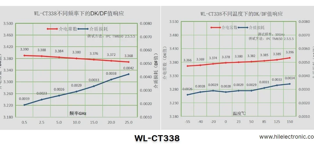
Custom WL-CT338 PCBs: Unlocking Performance for High-Tech Industries
At Highleap Electronic, we specialize in providing custom...

Custom Flex Board Production: Ultra-Long, Extra-Large, and Multi-Layer Designs
Flex boards, also known as flexible circuit boards (FPCs),...

Multilayer Flex PCB Manufacturing One-Stop Service
In today’s world of compact, high-performance, and...
How to get a quote for PCBs
Let us run DFM/DFA analysis for you and get back to you with a report.
You can upload your files securely through our website.
We require the following information in order to give you a quote:
-
- Gerber, ODB++, or .pcb, spec.
- BOM list if you require assembly
- Quantity
- Turn time
In addition to PCB manufacturing, we offer a comprehensive range of electronic services, including PCB design, PCBA (Printed Circuit Board Assembly), and turnkey solutions. Whether you need help with prototyping, design verification, component sourcing, or mass production, we provide end-to-end support to ensure your project’s success. For PCBA services, please provide your BOM (Bill of Materials) and any specific assembly instructions. We also offer DFM/DFA analysis to optimize your designs for manufacturability and assembly, ensuring a smooth production process.