
IoT PCB Assembly Cost Compliance and RF Integration

Figure 1. IoT PCB Assembly
Table of Contents
- IoT PCB Assembly Requirements: What Makes Connected Devices Different to Manufacture
- IoT PCB Assembly Cost Breakdown by Production Volume
- IoT Component Sourcing and BOM Risk Management
- FCC, CE, and RoHS: How Regulatory Requirements Affect Your Assembly Process
- RF and Antenna Assembly for Wireless IoT PCBs
- Scaling IoT PCB Production from Prototype to Volume
- Functional Testing for Battery-Powered IoT Devices
IoT PCB assembly covers everything from a 20 × 20 mm BLE sensor tag drawing 3 µA in sleep mode to a multi-board industrial gateway with cellular modem, Ethernet switch, and edge computing. What these products share is a combination of challenges that don’t exist in most other PCB categories: wireless RF performance that is sensitive to assembly decisions, battery life targets that depend on µA-level process cleanliness, regulatory certifications that are tied to specific production configurations, and volume ramps that move from 200-unit pilot to 50,000-unit production within 12 months. Engineers coming from consumer electronics or industrial control backgrounds routinely underestimate at least two of these — the result is schedule delays at certification, field failures from sleep-current leakage, or cost overruns from unplanned re-spins. This guide addresses the IoT-specific assembly decisions that determine whether the product reaches market on schedule and performs as designed in the field.
IoT PCB Assembly Requirements: What Makes Connected Devices Different to Manufacture
The Three Assembly Constraints Unique to IoT
1. RF performance is assembly-sensitive
Wireless devices have RF performance specifications (transmit power, receive sensitivity, antenna return loss) that are tested during regulatory certification and must be reproduced consistently in production. Assembly variables that most engineers don’t think of as RF issues — flux residue dielectric loading near the antenna, solder mask thickness variation in the antenna area, conformal coating thickness — all shift antenna resonant frequency and RF performance by measurable amounts. A device that passes bench testing and pre-compliance can fail regulatory certification if the production assembly introduces even small RF environment changes.
2. Battery life targets are µA-sensitive
A BLE sensor designed for 2-year CR2032 life draws perhaps 4 µA average. Ionic contamination from flux residue creates surface leakage paths of 0.5–3 µA per contaminated high-impedance node. Three contaminated nodes consume 1.5–9 µA — adding 37–225% to sleep current and cutting battery life by 27–70%. This failure mode is invisible to standard electrical test and AOI; it shows up only with µA-resolution current measurement at functional test.
3. Production configuration is tied to regulatory certification
FCC, CE, and other regulatory certifications test the final assembled product in its production configuration — specific PCB revision, specific firmware version, specific shielding and enclosure. Any assembly change after certification (different conformal coating type, different shielding can vendor, firmware update that changes RF duty cycle) may require re-test. This means assembly decisions made at prototype stage can have certification implications at volume production.
IoT Assembly Form Factor and Complexity Categories
| IoT Device Type | Typical BOM Cost | Primary Assembly Challenge | Critical Test Requirement |
|---|---|---|---|
| BLE/Zigbee sensor tag | $3–$8 | Sleep current leakage, antenna keep-out enforcement | Sleep current to ≤ 150% of target |
| LoRaWAN / NB-IoT node | $8–$25 | Module placement, thermal profile for modem IC | RF registration, sleep current |
| Wi-Fi + BLE combo | $6–$18 | Coexistence — shielding effectiveness | RF performance both bands, coexistence |
| Cellular gateway / hub | $25–$80 | Mixed THT+SMT, thermal management for cellular modem | Functional test across all interfaces |
IoT PCB Assembly Cost Breakdown by Production Volume
The Hidden Cost Layers Most Engineers Miss
Engineering business cases for IoT products typically model BOM + SMT labor + test. The actual unit cost includes several additional layers:
- Regulatory certification amortization: FCC ID + CE mark + IC Canada for a new radio product runs $15,000–$60,000. At 5,000 units, that’s $3–$12/unit. At 100,000 units it’s $0.15–$0.60/unit. Volume assumptions change economics dramatically.
- Conformal coating: Required for outdoor, industrial, and medical IoT. Selective spray coating with UV inspection adds $0.40–$1.20 per board — often missing from early assembly quotes.
- Per-unit firmware loading and serialization: Every cloud-connected device needs a unique device ID (MAC address, UUID, or serial number) programmed at production. In-line programming via SWD/JTAG/UART adds $0.20–$0.80 per unit — not optional for connected products.
- Component safety stock carrying cost: Long-lead BLE SoCs or cellular modules at 12–20 week lead time require 3-month safety stock. At $3.50/module, 10,000 units of buffer stock = $35,000 tied up in inventory — this is working capital, not manufacturing cost, but it’s real.
Assembly Cost by Volume Tier
| Volume | Assembly Cost / Board | Primary Cost Driver | Most Effective Cost Lever |
|---|---|---|---|
| 50–200 (prototype) | $25–$80 | NRE, minimum order quantities | Avoid re-spins — get DFM right first time |
| 500–2,000 (pilot) | $6–$18 | Test fixture setup, certification | Invest in functional test fixture now — pays back immediately |
| 5,000–20,000 | $2.50–$6 | Component pricing, yield loss | BOM optimization, approved alternates |
| 50,000+ | $0.80–$2.50 | Component cost, line efficiency | Long-term component contracts, dedicated line |
IoT Component Sourcing and BOM Risk Management
Why IoT SoC Availability Is Structurally Risky
IoT wireless SoCs (Nordic nRF52/53 series, Silicon Labs EFR32, Semtech SX1276, Quectel modules) are specialty semiconductors with lower production volumes than mainstream consumer chips. They are the first to go on allocation during supply tightening and the slowest to recover. The BLE chip designed in at prototype may carry 26-week lead time by volume production.
Best practices:
- Design in two approved sources for every critical active component — identify alternates at schematic stage, verify pin-compatibility, test firmware compatibility, and list all approved sources in the BOM before releasing for production.
- Module vs. discrete radio decision: Pre-certified modules (u-blox ANNA-B, Nordic nRF9160-DK, Quectel EC21) carry modular FCC/CE certifications that transfer to your end product. Discrete chipsets need full end-product certification. The break-even for discrete economics is typically 50,000–100,000 annual units. Below that threshold, modules win on total cost when certification is included.
- Screen for long-lead-time components before design freeze: Custom crystal frequencies, specialty MEMS sensors from single-source vendors, specific low-power PMICs — flag any component with >12 week lead time and evaluate alternatives before production volume is committed.
Passive Component Alternate Qualification
MLCCs, resistors, and inductors are commodity items. Secondary source alternates are almost always functionally equivalent for IoT applications operating below 3 GHz. Build a written alternate list and qualify it before the first production run. The assembly house should not be making BOM substitutions without a documented approval trail — unauthorized substitutions invalidate certification and void warranty claims.
A component sourcing service integrated with the assembly house provides lead-time monitoring across all BOM items and can source authorized alternates during shortages — significantly reducing schedule risk compared to purchasing components independently.

Figure 2. IoT PCB Assembly Board
FCC, CE, and RoHS: How Regulatory Requirements Affect Your Assembly Process
What Certification Actually Tests — and What Can Invalidate It
FCC and CE testing evaluates the final assembled product in its production configuration: the actual PCB revision, actual firmware, actual antenna, actual enclosure, actual cable routing. Assembly changes after certification may require re-test:
- Conformal coating type or thickness change: Coating adds dielectric loading near the antenna, shifting resonant frequency. The certified configuration specifies coating material and target thickness — deviating requires RF re-test.
- Shielding can change: Different can vendor, different installation method, or gap in perimeter solder seal changes EMC performance. Certification is specific to the configuration tested.
- Firmware version change: Some FCC grants are firmware-specific, particularly for devices with frequency hopping or adaptive power control. Maintain version control on production firmware.
- Cable routing inside enclosure: A USB cable routed parallel to the PCB antenna for 40 mm can couple enough RF to fail conducted emissions. This is a box-build assembly issue, not a PCB issue — but it shows up at EMC test.
RoHS Lead-Free Reflow Profiles and Heat-Sensitive IoT Components
RoHS-compliant lead-free assembly requires SnAgCu solder with peak reflow temperatures of 245–260°C. Many IoT components have limited thermal tolerance:
- MEMS sensors (accelerometers, gyros, barometers): many rated to 250°C maximum, some to 245°C
- Crystal oscillators: typically 260°C maximum, but time-above-liquidus must be controlled
- Coin-cell battery holders: mechanical parts with plastic ratings down to 230°C from some vendors
- Pre-certified wireless modules containing internal components: check module datasheet for max reflow temperature
Solution: profile with thermocouples on actual production boards before first production run. A standard textbook reflow profile is a starting point; the production profile must be validated specifically for your component mix, board mass, and oven characteristics.
IPC Class for IoT Products
Most commercial IoT devices ship to IPC Class 2 workmanship. Medical IoT with clinical claims (wearable ECG, continuous glucose monitors, fall detection with alert dispatch) requires Class 3 — tighter solder joint inspection, minimum copper plating thickness in vias, and formal first-article inspection documentation required for FDA submission. Class 3 adds 20–40% to assembly cost but is non-negotiable for FDA 510(k) and similar submissions.
RF and Antenna Assembly for Wireless IoT PCBs
PCB Antenna Keep-out Zone Enforcement
PCB-trace antennas (inverted-F, meander line, chip antenna with matching network) are highly sensitive to nearby copper, components, and dielectric loading. Assembly variables that shift antenna performance:
- Solder mask thickness variation in the antenna clearance area — solder mask has dielectric constant ~3.5, and thickness variations change effective permittivity
- Conformal coating applied over the antenna area — adds dielectric loading that shifts resonant frequency downward, typically by 3–8% for standard acrylic coating
- Shielding can edge proximity to the antenna ground plane
- Component placement tolerance near the antenna feedline
Keep-out zone violations should be caught during DFM review before fabrication. Any assembly process that modifies the RF environment (conformal coating, shielding can installation) should be RF-performance validated on the first production article.
Shielding Can Installation Quality
Shielding can effectiveness depends on a continuous ground seal around the can’s perimeter. A single gap in the solder joint creates a slot antenna that can actually worsen emissions at the gap’s resonant frequency. Inspection requirements:
- Visual inspection under magnification (10×) for solder continuity around the full perimeter
- Cross-section verification on first article to confirm intermetallic bond formation (not just surface wetting)
- RF test before and after shielding can installation on first production lot to confirm attenuation is as expected
Flux Residue and RF Performance
No-clean flux residue shifts the RF environment near traces and under shielding cans. For IoT products operating above 2.4 GHz, specify aqueous cleaning after reflow. The cost increment is $0.08–$0.25 per board. Compare this to the cost of EMC re-test ($5,000–$15,000) or field RF performance complaints.
Scaling IoT PCB Production from Prototype to Volume
The Prototype-to-Production Gap
IoT design validation prototypes are often hand-assembled or built on semi-manual lines. Volume production uses automated SMT assembly with stencil printing and reflow. These processes are not identical, and features that pass prototype testing sometimes fail in volume production:
- QFN thermal pads hand-soldered on prototypes have minimal voiding. Stencil-printed and reflowed QFN thermal pads often show 20–40% voiding if the stencil aperture isn’t window-paned — causing thermal resistance 2–3× higher than expected under load.
- Hand-placed 0201 passives never tombstone. Stencil-deposited paste with asymmetric volume tombstones at 1–5% rate if pad thermal balance isn’t designed in.
- Antenna keep-out zones respected by hand assembly but violated by automated placement if the placement program has a coordinate offset error.
First Production Article Qualification Protocol
Bridging the prototype-to-production confidence gap requires a structured qualification program before volume commitment:
- Build 10–20 units using full production tooling — stencil, pick-and-place, reflow profile, selective wash
- Run full functional test including sleep current measurement and RF performance
- Cross-section 2–3 boards: QFN thermal pad voiding, microvia barrel copper thickness, solder joint intermetallic formation
- Run 50-cycle thermal shock (−40°C to +85°C) on 5 boards to detect latent solder joint fatigue
- Document all results as the production baseline; sign off before scaling volume
This adds 2–3 weeks and $3,000–$8,000. It prevents $50,000–$500,000 in field return costs from a production defect that wasn’t visible at prototype.
Functional Testing for Battery-Powered IoT Devices
Sleep Current Testing: Why It Must Be a Production Test
Sleep current is the single most important performance specification for battery-powered IoT devices. It is affected by assembly quality in ways standard electrical test and AOI do not detect:
- Ionic contamination: Flux residue between high-impedance MCU pins creates leakage of 0.5–3 µA per contaminated node. A device designed for 4 µA sleep with three contaminated nodes draws 5.5–13 µA — battery life drops from 2 years to 8 months.
- Component substitution: An alternate MOSFET or LDO with higher gate/quiescent leakage than the designed part adds µA that appear only at sleep-state measurement.
- ESD or thermal damage: Assembly damage to the MCU can disable sleep mode gating — the peripheral clock keeps running, drawing 500 µA in “sleep” instead of 4 µA. This is undetectable by visual inspection or continuity test.
Every IoT board should be tested for sleep current at the functional test station. The measurement requires:
- 100 nA-resolution ammeter in series with the supply (1 µA resolution minimum; 100 nA preferred for ultra-low-power designs)
- Firmware test sequence that cycles through wake/operate/sleep and holds in sleep for 5 seconds
- Pass/fail limit: ≤ 150% of design target sleep current (e.g., if designed for 4 µA, fail anything above 6 µA)
The test adds 8–15 seconds per board. At $0.15 per second in functional test cost, that is $1.20–$2.25 per board — trivially small compared to a field return from premature battery failure.
Firmware Programming and Serialization at Production
Every IoT device must ship with production firmware and a unique device identifier. In-line ISP programming at the functional test station programs firmware and burns the device serial number, MAC address, or cloud credentials simultaneously with functional verification. This is not optional — devices that ship without unique IDs cannot be provisioned, managed, or updated over the air.
Highleap’s IoT Assembly Platform
Highleap Electronics provides full IoT assembly support from prototype through volume production:
- RF-aware processes: DFM review includes antenna keep-out zone audit; RF first-article performance test with return loss measurement; shielding can perimeter inspection
- Sleep current test: 100 nA-resolution current measurement at functional test; standard on all battery-powered IoT orders
- Firmware programming: In-line SWD/JTAG/UART ISP with per-unit serial number provisioning and cloud traceability
- Conformal coating: Selective spray with UV fluorescent inspection; acrylic, urethane, and silicone materials available
- Component sourcing: Lead-time screening on every BOM; authorized alternate qualification support; 500,000+ part database across Nordic, Silicon Labs, Quectel, u-blox, Semtech platforms
- Volume range: 50-unit prototypes through 100,000-unit annual production — no partner change required at scale-up

Recommended Posts
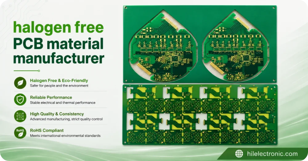
Halogen Free PCB Material Manufacturer for Compliant PCB Fabrication and Assembly
Halogen free PCB material manufacturing is usually a...
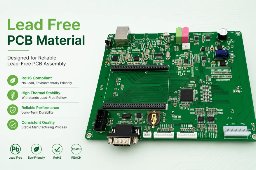
Lead Free PCB Material for PCB Assembly and Reliable PCBA Manufacturing
Lead free PCB material selection belongs in the assembly...
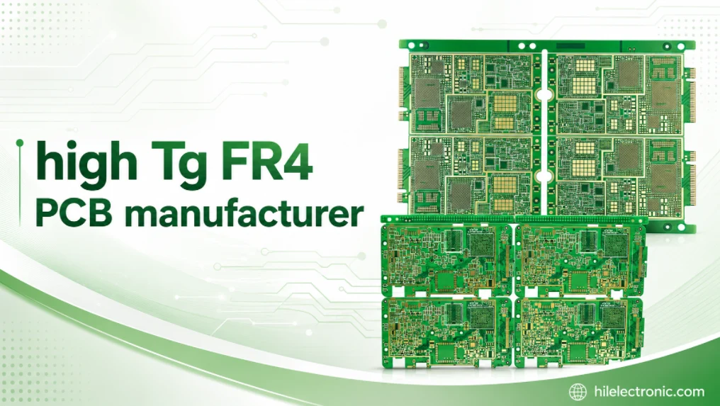
High Tg FR4 PCB Manufacturer for Industrial, Automotive, and Power Electronics
High Tg FR4 PCB manufacturing is usually driven by a...
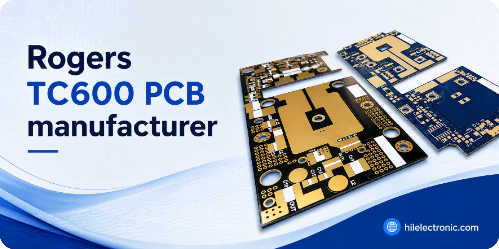
Rogers TC600 PCB Manufacturer for High-Dk and High Thermal Conductivity RF Boards
Rogers TC600 PCB manufacturing is usually requested when a...
How to get a quote for PCBs
Let‘s run DFM/DFA analysis for you and get back to you with a report. You can upload your files securely through our website. We require the following information in order to give you a quote:
-
- Gerber, ODB++, or .pcb, spec.
- BOM list if you require assembly
- Quantity
- Turn time
For PCBA services, please provide your BOM (Bill of Materials) and any specific assembly instructions. We also offer DFM/DFA analysis to optimize your designs for manufacturability and assembly, ensuring a smooth production process.