
PCB Drilling Design Rules for Reliable PCB Manufacturing

PCB drilling is not just a hole-making step in board fabrication. It is one of the most important manufacturing stages affecting electrical reliability, component fit, plating quality, stack-up registration, CAM optimization, and total production cost. For engineers, drill design directly affects whether a PCB is easy to manufacture, whether via structures are reliable, and whether the final board can meet both performance and budget targets. For CAM engineers, drill files, tool size selection, hole tolerance, and hole count all influence how efficiently the job can be processed and how much manufacturing risk is introduced before production even begins.
At Highleap Electronics, we support drilling-intensive designs through PCB fabrication for standard multilayer boards, HDI structures, industrial electronics, communication products, and other complex designs where drilling quality is critical to yield and long-term reliability. This guide explains PCB drilling from the perspective of design, CAM engineering, manufacturability, and cost control, so engineers can make better decisions before release to fabrication.
Table of Contents
- Why PCB Drilling Matters More Than Most Designers Expect
- PCB Hole Types and Their Manufacturing Purpose
- Minimum Drill Size, Finished Hole Size, and Drill Compensation
- Hole Tolerance, Position Accuracy, and Annular Ring Control
- Mechanical Drilling vs Laser Drilling
- How CAM Engineers Optimize PCB Drill Files
- How Hole Count and Tool Changes Affect Cost and Lead Time
- Common PCB Drilling Problems and How to Prevent Them
- DFM Rules for Better PCB Drilling Design
- PCB Drilling FAQ
Why PCB Drilling Matters More Than Most Designers Expect
PCB drilling affects much more than whether a hole appears in the right place. In modern board manufacturing, drilled holes are often part of the electrical structure, the assembly structure, and the mechanical structure of the product at the same time. A poor drilling decision at the design stage can cause annular ring breakout, plating weakness, hole wall damage, registration failure, unnecessary tool changes, higher scrap risk, and avoidable cost increases.
For example, a via that is electrically acceptable in the schematic may still be expensive or risky in production if the drill size is too small, the aspect ratio is too high, or the annular ring is too narrow. In the same way, a design with too many non-standard drill tools may increase CAM complexity and production time without providing any real electrical benefit.
This is why drilling should never be treated as a minor output file detail. It is a core DFM topic that influences fabrication quality, reliability, and cost from the beginning.
PCB Hole Types and Their Manufacturing Purpose
Different hole structures are used in PCB manufacturing for different electrical and mechanical needs. Each type also creates different manufacturing requirements.
- Plated through-hole (PTH): drilled through the full board thickness and later copper plated. Used for through-hole components and full-depth interlayer electrical connections.
- Non-plated through-hole (NPTH): mechanical hole without copper plating. Used for mounting, tooling, or alignment features.
- Blind via: connects an outer layer to one or more internal layers without passing through the full board.
- Buried via: located completely between inner layers and invisible from the outer surface.
- Microvia: very small laser-drilled via, typically used in HDI PCB designs to connect adjacent layers.
- Back drill hole: controlled-depth hole used to remove via stubs in high-speed designs.
- Slotted hole: elongated mechanical or plated opening used for connectors, terminals, or mechanical fit requirements.
These hole types may look similar in output files, but they are not processed the same way in manufacturing. That is why drill data must clearly distinguish plated and non-plated holes, finished hole requirements, and any controlled-depth or sequential build structures.
Minimum Drill Size, Finished Hole Size, and Drill Compensation
One of the most important topics for engineers is the relationship between drill size and finished hole size. The hole defined in the design is often the required finished size, not the actual drill bit size used in fabrication.
This matters because plated holes become smaller after drilling due to copper deposition and process effects. To achieve the target finished hole, the actual drill tool usually needs to be larger than the required final size.
Typical design considerations include:
- Finished hole size: the final usable diameter after plating
- Drill compensation: the extra drill diameter needed to achieve the finished hole target
- Board thickness: thicker boards create greater drilling and plating challenges
- Aspect ratio: the ratio of board thickness to drilled hole diameter
| Hole Category | Typical Manufacturing Range | Notes |
|---|---|---|
| Standard mechanical PTH | Commonly around 0.20 mm and above | Used for most standard vias and through-hole parts |
| Fine mechanical drill | Below common standard range | Higher risk, more tool sensitivity, more cost |
| Laser microvia | Much smaller than mechanical via | Used in HDI sequential build-up structures |
| Large mechanical mounting hole | Depends on connector and hardware needs | Often NPTH and mechanically driven |
In real projects, the best practice is not to push drill size as small as possible just because the design tool allows it. The correct question is whether the hole size is necessary, manufacturable, and cost-effective for the stack-up and reliability target.
Hole Tolerance, Position Accuracy, and Annular Ring Control
Hole size alone is not enough. Engineers also need to understand tolerance and registration. Even if the nominal hole diameter is correct, the finished result can still fail if the hole is off position or too close to the edge of the pad.
Important control points include:
- Finished hole tolerance: determines whether component leads, press-fit pins, and mechanical parts will fit correctly
- Hole position tolerance: determines whether the hole stays centered inside the pad
- Annular ring: the copper ring remaining around the drilled hole after manufacturing tolerances are applied
- Breakout risk: occurs when the drilled hole shifts too close to or beyond the pad boundary
For CAM engineers, this is where design review becomes critical. Hole diameter, pad size, tolerance stack-up, and layer registration must all be checked together. A design with aggressive hole sizes and weak annular ring may pass a simple CAD check but still create a serious yield risk in manufacturing.
If the board includes precision RF lines or back-drilled structures, those tolerance decisions also interact with the wider high-frequency PCB design strategy.
Mechanical Drilling vs Laser Drilling
Most PCB holes are still made by mechanical drilling, but laser drilling is essential for many HDI structures. Choosing between them is not just a technology preference. It affects via type, layer strategy, cost, and manufacturability.
| Method | Best For | Main Advantage | Main Limitation |
|---|---|---|---|
| Mechanical drilling | Through-holes, standard vias, mounting holes, slots | Widely used, efficient, suitable for most boards | Limited by drill bit size and tool wear |
| Laser drilling | Microvias, HDI build-up layers, very small via structures | Supports fine-pitch and high-density interconnection | Higher process cost and more complex stack-up planning |
Mechanical drilling remains the mainstream solution for standard multilayer boards. Laser drilling becomes necessary when interconnect density exceeds what mechanical drills can support economically or reliably.
How CAM Engineers Optimize PCB Drill Files
This is one of the most overlooked parts of PCB drilling from the customer side. The drill file is not just a passive output. It is one of the main CAM optimization points in the engineering workflow.
Before release to production, CAM engineers typically review:
- Tool size consolidation: whether similar hole sizes can be combined safely to reduce tool count
- PTH vs NPTH separation: whether plated and non-plated holes are clearly defined
- Finished hole vs drill size logic: whether the design intent matches real manufacturing compensation
- Hole count by tool: whether a given drill size creates an excessive tool load or unusual cycle time
- Slot and special hole processing: whether slots, countersinks, or controlled-depth holes need special routing or drilling treatment
- Annular ring verification: whether the selected tool sizes will remain manufacturable after tolerance is applied
Good CAM optimization improves more than just manufacturability. It can reduce drill tool changes, shorten production time, lower tooling stress, improve yield, and help stabilize cost. Poor drill data does the opposite: more tools, more complexity, more review time, and more production risk.
That is also why drilling rules should be checked during PCB design, not only after Gerber and drill files are already finalized.
How Hole Count and Tool Changes Affect Cost and Lead Time
Many engineers think cost comes mainly from board size, layer count, and surface finish. In reality, drilling can also have a strong cost impact, especially on complex boards.
The main cost drivers related to drilling include:
- Total hole count: more holes mean longer machine time
- Number of drill tools: more tool diameters mean more setup and more CAM complexity
- Small-hole percentage: finer holes increase process sensitivity and may require slower production conditions
- Stack-up thickness: thicker boards make drilling and plating more difficult
- Back drilling or controlled-depth drilling: adds process complexity
- HDI microvia content: usually increases fabrication cost significantly
For cost control, one of the best design habits is to avoid unnecessary drill size variation. If two hole sizes serve the same practical function, standardizing them can simplify both CAM work and production.
Common PCB Drilling Problems and How to Prevent Them
Drilling defects often do not appear as “drilling defects” to the customer. Instead, they may show up later as plating failure, open circuits, breakout, assembly fit problems, or unreliable vias in thermal cycling.
Common problems include:
- Drill wander: the hole deviates from its intended center due to material behavior or drilling conditions
- Breakout: the hole edge cuts too close to or beyond the pad boundary
- Smear: resin residue remains on hole walls and affects subsequent metallization
- Rough hole wall: reduces plating reliability and increases interconnect risk
- Drill breakage: especially with small tools, deep drilling, or poor chip evacuation
- Burrs or debris: can affect cleanliness and later process stability
Most of these problems are reduced by a combination of better design rules, better CAM review, correct drilling parameters, and realistic manufacturing allowances.
DFM Rules for Better PCB Drilling Design
If the goal is better manufacturability, lower cost, and higher drilling reliability, these rules matter:
- Use the largest practical drill size: do not choose small holes unless the design truly requires them
- Maintain enough annular ring: give the drill process realistic positional tolerance room
- Standardize tool sizes where possible: fewer drill tools usually mean easier CAM optimization and better efficiency
- Separate plated and non-plated holes clearly: never make CAM guess
- Match hole structure to stack-up: do not force through-holes where microvias or sequential build structures are more appropriate
- Review aspect ratio early: especially for thick boards and small plated holes
- Consider the final assembly need: connector fit, press-fit tolerance, and pin insertion all depend on realistic finished hole control
Engineers who treat drilling as part of DFM—not just part of CAD output—usually get faster prototype approval, cleaner CAM review, better yields, and more stable board performance. If you are validating a new design, starting with a prototype PCB build is often the best way to confirm that drill structures, hole tolerances, and stack-up decisions are all manufacturable before volume release.
Get a Quote for Your PCB Drill Design
PCB Drilling FAQ
What is the difference between drill size and finished hole size in PCB manufacturing?
Drill size is the physical tool diameter used during fabrication. Finished hole size is the final diameter after plating and processing. For plated holes, the finished diameter is usually smaller than the original drill diameter.
What is the typical minimum drill size for a standard PCB?
That depends on the board structure, thickness, and manufacturer capability, but standard mechanical drilling is usually larger than HDI microvia structures. Very small holes are possible, but they increase manufacturing difficulty and cost.
Why does hole count affect PCB cost?
Because drilling time, tool changes, small-hole handling, and CAM complexity all increase as hole count and drill variety increase.
Why is CAM review important for PCB drill files?
Because CAM engineers verify tool sizes, plated vs non-plated hole definitions, annular ring safety, manufacturability, and optimization opportunities before the board enters production.
When should laser drilling be used instead of mechanical drilling?
Laser drilling is mainly used for microvias and HDI designs where hole sizes are too small or too dense for practical mechanical drilling.

Related Articles
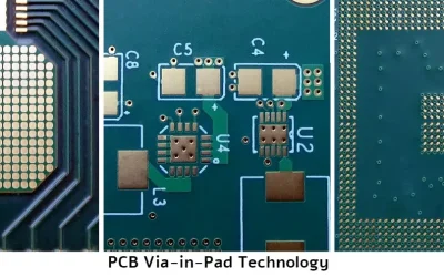
Comprehensive Analysis of PCB Via-in-Pad Technology
Explore the key advantages and challenges of Via-in-Pad technology in PCB design, with expert tips for maximizing performance and reliability.
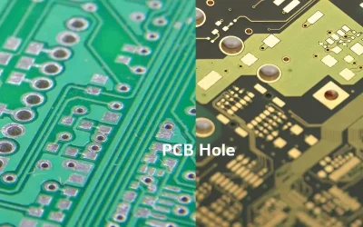
PCB Hole Selection to Optimize PCB Performance and Cost
Discover how to optimize your PCB designs with effective hole selection techniques like back drilling vs buried vias, mechanical vs laser drilling, and HDI stack planning to improve performance while minimizing manufacturing complexity and costs.
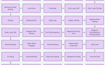
PCB Manufacturing Process Flow – Ultimate Guide Is Here
High-Quality PCB Manufacturing Solutions: Precision, Speed, and Reliability for Your Electronics Projects – From Prototype to Mass Production.
Take a Quick Quote