
How to Test a Circuit Board: PCB and PCBA Methods

Circuit Board Testing — Quick Reference
- Stage 1 — Visual inspection: Burns, cracks, lifted pads, solder bridges, swollen capacitors — no instruments needed, catches 30–40% of failures
- Stage 2 — Power rail verification: Multimeter DC voltage measurement against design spec; check before applying power to unfamiliar boards
- Stage 3 — Continuity testing: Multimeter continuity mode; verify trace integrity, check suspected open circuits and solder joints
- Stage 4 — Component-level testing: Resistance, diode forward voltage, capacitor ESR — identify failed individual components in-circuit or out-of-circuit
- Stage 5 — Signal integrity testing: Oscilloscope; verify clock signals, communication bus waveforms, and power supply ripple
- Stage 6 — Functional testing: Apply inputs, verify outputs; confirm the board performs its intended function end-to-end
Need a PCB Built and Tested? Get a Quote →
This page is the general testing hub. For low-volume or fixtureless checks, use flying probe testing; for assembled boards, connect the test plan with PCBA functional testing; for bare-board continuity and isolation, use PCB electrical testing.
Table of Contents
- Tools Needed for Circuit Board Testing
- Stage 1: Visual Inspection — What to Look For and Where
- Stage 2: Power Rail Testing with a Multimeter
- Stage 3: Continuity Testing — Tracing Open Circuits and Bad Joints
- Stage 4: Component-Level Testing (Resistors, Capacitors, Diodes, Transistors)
- Stage 5: Oscilloscope Testing for Signal Integrity
- Stage 6: Functional Testing and Output Verification
- Most Common PCB Failure Modes and How to Identify Them
- How Professional PCB Factories Test Circuit Boards
- Frequently Asked Questions
Tools Needed for Circuit Board Testing
Different stages of circuit board testing require different instruments. Using the right tool at each stage is not a matter of preference — each instrument measures something different, and no single tool covers all failure modes.
Digital multimeter (DMM)
The essential starting instrument for circuit board testing. A good DMM measures DC and AC voltage, DC and AC current, resistance, continuity (with audible beep), diode forward voltage, and often capacitance and frequency. For PCB testing, the minimum specifications you want are: 0.5% DC voltage accuracy or better; a continuity mode that beeps in under 200ms (slow-responding multimeters miss intermittent faults); and a current input protected to at least 200mA with a separate fused input for ampere-range measurements. True RMS measurement matters when measuring AC signals on switching power supplies where the waveform is not sinusoidal.
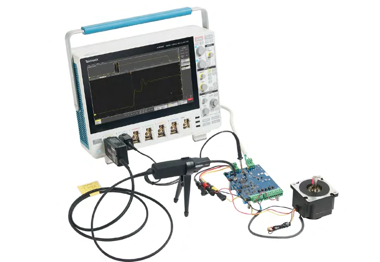
Oscilloscope
An oscilloscope displays voltage as a function of time, making it the correct tool for any test where waveform shape, timing, or frequency matters. For circuit board testing, a two-channel digital oscilloscope with at least 100 MHz bandwidth covers most embedded electronics and power supply testing. Bandwidth needs to be at least 5× the highest frequency signal you expect to capture accurately. For digital communication buses (SPI, I2C, UART, CAN), a 4-channel oscilloscope with protocol decoding is significantly more useful than a 2-channel model. A 20 MHz oscilloscope is only adequate for power supply ripple and low-frequency signals — it will not correctly show the ringing and overshoot on fast digital edges.
LCR meter or component tester
A dedicated LCR (Inductance-Capacitance-Resistance) meter measures component values more accurately than a multimeter, particularly for capacitors where ESR (Equivalent Series Resistance) is often more diagnostically useful than capacitance value. High ESR is the most common failure mode in electrolytic capacitors and will not be caught by capacitance measurement alone.
DC power supply with current limiting
When testing a repaired or suspect board for the first time, powering it from a current-limited bench supply instead of the production power source allows you to set a current limit just above the expected idle current. If a short is present, the supply will limit and display the fault current rather than allowing the short to overheat components.
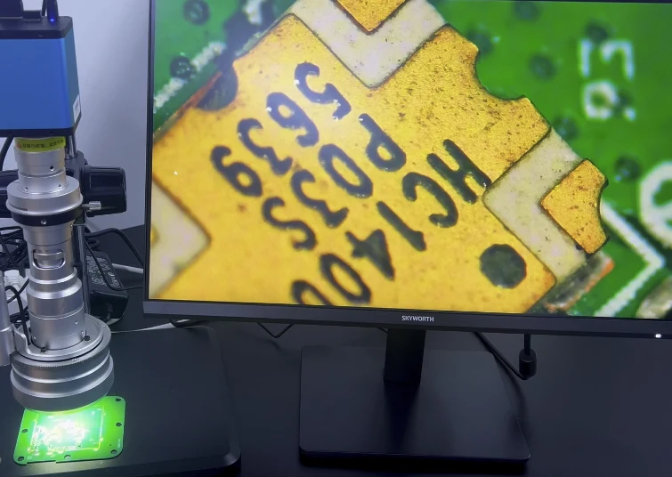
Inspection microscope or digital microscope
Fine-pitch SMD solder joints, 0402 and smaller passive components, and BGA solder ball inspection require magnification that a hand-held loupe cannot provide reliably. A digital microscope with on-screen display allows you to inspect while keeping both hands free.
Supplementary instruments
Logic analyzer: captures and decodes digital signals on multiple channels simultaneously — far more useful than an oscilloscope for debugging SPI, I2C, UART, USB, or CAN communication where you need to read the actual data content. Function generator: applies test signals to specific nodes, allowing you to characterize filter response, amplifier gain, or signal path integrity. Thermal camera or thermal imaging phone attachment: identifies overheating components that are not yet visibly damaged.
Stage 1: Visual Inspection — What to Look For and Where
Visual inspection is the fastest and cheapest testing stage, and it catches a surprising proportion of circuit board failures — industry data suggests 30–40% of board failures have a visible cause. The technique requires no instruments, just good lighting, magnification, and a systematic approach.
Burned or scorched areas
Brown or black discoloration on the PCB surface around a component indicates that component has dissipated more heat than it was designed for. This usually means either an overloaded resistor, a shorted power transistor or MOSFET, or a failed voltage regulator. Note the exact location and check the schematic to identify what function that component performs and what could have caused the overload condition. Do not assume the burned component is the root cause — it may have failed because another component failed first, pushing excess current through it.
Swollen or leaking capacitors
Electrolytic capacitors fail by internal gas buildup that causes the top of the can to dome or bulge. In severe cases, the vent seal at the top ruptures and electrolyte leaks onto the PCB surface. A swollen capacitor is definitively failed and must be replaced. Check nearby capacitors too — capacitor failure in one area of a power supply often indicates a systemic issue (overvoltage, excessive ripple, or incorrect capacitor voltage rating) that affects all capacitors in that section.
Solder bridges
A solder bridge is a small blob of solder connecting two adjacent pads or leads that should not be electrically connected. Bridges on fine-pitch ICs (0.5mm pitch QFP or QFN packages) are too small to see without magnification. Solder bridges cause dead shorts between pins — the resulting symptoms depend entirely on which pins are bridged: a bridge between adjacent signal pins may cause intermittent malfunction; a bridge between a power and ground pin will blow the power supply fuse or destroy the IC immediately.
Cold solder joints
A cold solder joint forms when the solder solidifies before fully wetting both the component lead and the pad. Cold joints appear dull and grainy rather than smooth and shiny; they often have a concave or cracked appearance rather than the smooth meniscus of a good joint. Cold joints have high resistance that may be intermittent — the joint passes continuity testing when cold but opens when warmed by component self-heating in operation. Under magnification, look for the characteristic grainy texture and irregular shape.
Lifted pads and broken traces
Physical damage from mishandling, rework, or thermal stress can lift a pad from the PCB substrate, breaking the connection to the trace underneath. Lifted pads appear as pads that are slightly raised or separated from the board surface, often with the trace still attached to the pad rather than the board. Broken traces are less common but occur at stress points near board edges, near large heavy components that create leverage, or at areas exposed to repeated flexing. Use a magnifier to check trace continuity visually before probing electrically.
Cracked components
Ceramic capacitors and resistors can crack from thermal shock, mechanical stress, or incorrect handling. A cracked ceramic capacitor may appear identical to an undamaged one visually, but sometimes a crack line is visible under magnification. The failure mode is open-circuit or intermittent open. Check component bodies at board flexion points and near any area showing signs of mechanical stress.
Stage 2: Power Rail Testing with a Multimeter
Power rail verification confirms that the board is receiving the correct input voltage and distributing the correct regulated voltages to each section of the circuit. Power rail failures account for a large proportion of total circuit board failures because they affect every component supplied by the failed rail.
Procedure: measuring DC supply rails
Set the multimeter to DC voltage mode, range set to above the expected voltage. Place the black probe on a known good ground point — the ground pin of a connector, the negative terminal of an electrolytic capacitor, or the exposed copper ground pour if accessible. Place the red probe on each power test point in sequence.
Expected readings: the measured voltage should be within ±5% of the nominal voltage for most digital logic supplies (3.3V, 5V, 12V). Precision analog circuits may require ±1–2% regulation. A reading of 0V on a rail that should be active means either the power supply is not providing voltage, the linear regulator or DC-DC converter on that rail has failed, or there is a short circuit pulling the rail to ground. A reading significantly lower than nominal (for example, 3.1V on a 5V rail) suggests a high-resistance fault, an overloaded regulator, or a regulator entering current limiting due to an excessive load.
Checking for supply shorts before power-on
Before applying power to an unknown or suspect board, measure resistance between each supply rail and ground with the board unpowered. On most circuit boards, you will see a finite resistance (typically 10 kΩ to several MΩ) from power to ground because of pull-down resistors and the input impedance of ICs. A reading below approximately 100 Ω from a power rail to ground indicates a short circuit that should be investigated before applying power. Exceptions: boards with large bulk capacitance will initially read near-zero and then rise as the capacitor charges from the multimeter’s test current — this is normal.
Voltage regulator testing
Linear voltage regulators (LDO regulators) have three terminals: input, output, and ground/adjust. With power applied, measure the input voltage (should be above the dropout voltage of the regulator), then measure the output voltage (should match the regulator’s rated output). A regulator that shows correct input but incorrect output is failed or incorrectly connected. A regulator that shows correct output at no load but incorrect output under load is either undersized for the current demand or is thermally shutting down.
Ripple measurement
Switching power supplies and DC-DC converters produce output voltage ripple — a small AC variation superimposed on the DC output. Excessive ripple indicates a failing output capacitor, an inductor out of specification, or a feedback loop problem. To measure ripple, set your multimeter to AC voltage mode while the supply operates; ripple should typically be less than 1% of the nominal output voltage. For more accurate ripple measurement, use an oscilloscope set to AC coupling with the timebase set to capture several switching cycles.
Stage 3: Continuity Testing — Tracing Open Circuits and Bad Joints
Continuity testing verifies that a conductive path exists between two points that should be connected. The multimeter continuity mode passes a small test current through the circuit and beeps if the resistance is below a threshold (typically 30–100 Ω depending on the meter). Continuity testing is the correct method for checking suspected open solder joints, broken traces, blown fuses, and connector contacts.
Testing solder joint continuity
Place one probe on the component lead and the other probe on the trace connected to that pad (not on the pad itself). If the solder joint is good, you will hear the beep immediately. If the joint is open, you will get no beep even though the component lead may appear to be sitting on the pad. For through-hole components, probe the component lead on the top side and the corresponding trace on the bottom side — an open joint will show no continuity between them even with the component physically inserted.
Tracing broken traces
If a node tests as open when it should be connected, systematically trace the connection using the schematic. Start at one end of the suspected trace and check continuity to intermediate test points moving toward the other end. The point where continuity fails locates the break. Under-board traces can break invisibly at board flex points; if the break is confirmed electrically but not visible, gently flex the board while holding the probes on either side of the suspected location — an intermittent break will appear and disappear as the board flexes.
Checking for unintended shorts
Continuity testing also identifies shorts — connections between points that should be isolated. For adjacent pins on an IC, set the multimeter to resistance mode rather than continuity mode (the continuity beep may sound for paths with a few hundred ohms that are not true shorts). For adjacent power and ground pads on connectors, any resistance below a few kilohms warrants investigation.
Testing connectors and fuses
Connectors are common failure points from repeated mating cycles, contamination, or bent pins. Test each connector pin to its corresponding PCB pad with continuity mode. For fuses, a good fuse reads near-zero resistance (continuity beep); a blown fuse reads open. Test fuses in-circuit with the power supply disconnected to avoid parallel paths confusing the reading.
Stage 4: Component-Level Testing (Resistors, Capacitors, Diodes, Transistors)
Component-level testing identifies which specific component has failed. Most components can be tested in-circuit with the power removed, though parallel paths in the circuit may affect readings. When in doubt, desolder one end of the component to break it out of the circuit before measuring.
Resistors
Set the multimeter to resistance mode. With power removed from the board, measure the resistance across the resistor. A good resistor reads within ±5% of its marked value (for standard 5% tolerance components) or ±1% for precision components. A reading significantly higher than marked value indicates a partial open — internal resistance has increased, common in high-wattage wire-wound resistors after overload. A reading of zero indicates a short. A reading of infinite (open) indicates a complete failure of the resistive element, usually from overheating.
Caution: in-circuit resistance measurements are affected by parallel paths through other components. If the reading seems wrong, check the schematic for parallel components before concluding the resistor is faulty.
Capacitors
Simple capacitance measurement with a multimeter is often insufficient for diagnosing capacitor failure. Capacitors fail primarily by increased ESR (equivalent series resistance) rather than loss of capacitance. A capacitor with 10× its normal ESR will still measure close to its rated capacitance value but will not filter ripple effectively, causing symptoms that look like a power supply problem.
To test ESR: use a dedicated ESR meter or LCR meter with ESR measurement capability. Discharge the capacitor completely before measurement. For through-hole electrolytic capacitors, ESR values below 0.5 Ω are typically acceptable; values above 1–2 Ω indicate a failing capacitor. For testing with a multimeter in the absence of an ESR meter: charge the capacitor briefly from the supply, then switch to resistance mode and watch the reading — a good capacitor will show a high but finite reading that slowly increases as the capacitor discharges into the meter; a shorted capacitor reads near-zero; an open capacitor reads immediately infinite.
Diodes and Schottky diodes
Set the multimeter to diode test mode. Place the red probe on the anode and black probe on the cathode. A good silicon diode reads 0.5–0.7V forward voltage. A Schottky diode reads 0.2–0.4V. A reading of zero indicates a short (diode has failed short-circuit, common under reverse voltage stress). A reading of OL (overload) in both orientations indicates an open diode. For in-circuit diode testing, note that parallel components may affect the reading — a forward voltage reading significantly below the expected value may indicate a parallel low-resistance path rather than a failed diode.
Transistors (BJT)
A bipolar transistor can be tested as two back-to-back diodes. For an NPN transistor: red probe to base, black probe to emitter should show ~0.6–0.7V forward voltage; red to base, black to collector should also show ~0.6–0.7V. All other combinations should show open (OL). A reading of zero in any combination indicates a short between those junctions. For PNP, reverse the probe polarity. A transistor that tests correctly as individual junctions but fails in circuit may have degraded gain (hFE) rather than a junction failure — use the hFE test socket on a multimeter or component tester to verify gain.
MOSFETs
MOSFETs are more difficult to test in-circuit because the gate-drain capacitance can hold a charge that affects measurement. With power removed, short the gate to source to discharge any stored charge. Then measure drain-to-source resistance: it should be very high (megohms) for an N-channel FET with VGS = 0. Apply a small voltage (typically 5V) gate-to-source from a bench supply, then recheck drain-source resistance — it should drop dramatically. A MOSFET that shows low drain-source resistance with gate shorted to source has failed short-circuit. A MOSFET that fails to switch on with VGS applied has an open gate or degraded threshold voltage.
Stage 5: Oscilloscope Testing for Signal Integrity
An oscilloscope is required for any circuit board testing that involves signals varying in time — clock signals, digital data buses, PWM outputs, analog sensor signals, and power supply switching waveforms. A multimeter’s DC or AC voltage readings cannot reveal signal shape, timing, noise, or protocol content.
Power supply ripple and noise
Connect the oscilloscope probe to a power rail with AC coupling enabled. Set the vertical scale to 50–100 mV/division. Set the timebase to capture several switching cycles of the power supply (for a 100 kHz switching frequency, set approximately 2–5 µs/division). Good power supply output should show ripple below 1% of the nominal voltage for digital circuits; below 0.1% for precision analog circuits. Excessive ripple that increases at higher load current indicates a failing output capacitor. High-frequency noise spikes that do not relate to the switching frequency may indicate poor decoupling or a layout problem.
Clock signal verification
Crystal oscillators and clock ICs produce the timing reference for all synchronous digital circuits. Set the oscilloscope to trigger on the clock signal. A healthy clock should show a clean square wave (or sine wave for crystal oscillator output before the buffer) with rise and fall times appropriate for the signal frequency. Missing clock signal: the crystal has failed, the oscillator circuit has a component fault, or the load capacitance is out of specification. Distorted clock: may indicate incorrect load capacitance, a failing crystal, or excessive loading from driven circuits. Verify the clock frequency against the crystal or oscillator part number marked on the component.
Digital communication bus testing
For SPI, I2C, UART, CAN, and similar buses, the oscilloscope verifies that signals are present and at the correct voltage levels. Use the protocol decode function if available: this displays the decoded data alongside the waveform, allowing you to see not just whether signals are present but whether the correct data is being transmitted. Key checks for each bus type:
SPI: verify chip select goes low during transactions, clock is present and at the correct frequency, MOSI and MISO toggle during data transfer. I2C: verify start condition (SDA falling while SCL high), correct address byte, ACK bits. UART: verify baud rate (count bits per second), 8N1 or other framing, correct idle high state. CAN: verify differential signaling on CANH/CANL, dominant/recessive states, frame structure.
Analog signal testing
For sensor inputs and analog processing stages, the oscilloscope verifies signal amplitude, frequency, and absence of noise that would corrupt analog-to-digital conversion. Key measurements: verify the signal spans the expected range without clipping; check for noise floor (random variation in the signal when the input should be constant); identify any periodic interference at the power supply switching frequency that is coupling into the analog path.
Stage 6: Functional Testing and Output Verification
Functional testing confirms that the board performs its intended function correctly — not just that individual components test within spec, but that the integrated system produces correct outputs for known inputs. This is the final stage of testing and the only stage that can reveal system-level failures that component-level testing misses.
Defining the test specification
Before functional testing begins, you need to know what the board is supposed to do: what inputs it accepts, what outputs it produces, what the correct output looks like for each input state, and what the timing requirements are. For boards with a schematic, this information comes from the functional description. For boards without documentation, reverse engineering the function from the schematic and component datasheets is necessary before meaningful functional testing is possible.
Input stimulus and output measurement
Apply each input condition that the board is designed to handle and verify the corresponding output. For digital control boards: apply the defined input signals and verify that outputs switch correctly and within the specified timing. For analog processing boards: apply a calibrated input from a function generator and measure the output with the oscilloscope to verify gain, frequency response, and noise performance. For power supply boards: apply the rated input voltage and load, then verify output voltage regulation over the full load range from no-load to maximum rated current.
Boundary condition testing
Test at the edges of the specified operating range, not just at nominal conditions. A board that works correctly at 25°C room temperature may fail at 70°C operating temperature or at the low end of its supply voltage range. Boundary testing is particularly important for boards returning from field service with intermittent complaints that do not reproduce at room temperature.
Automated functional test (bed-of-nails)
For production volume testing, manual probing is replaced by a bed-of-nails fixture — a custom fixture with spring-loaded pins that contact test points on the board surface simultaneously. A test program then applies stimuli and checks responses automatically, verifying every test point in the specification within seconds. This approach is what professional PCB assembly factories use for production testing; it provides complete coverage and a documented pass/fail record for every board in the production run.
Most Common PCB Failure Modes and How to Identify Them
Understanding the most frequent circuit board failure modes helps you prioritize which tests to run first. Different failure modes produce different symptoms, and targeting your testing based on the observed symptom saves significant diagnostic time.
How Professional PCB Factories Test Circuit Boards
Understanding how professional PCB assembly factories test boards provides context for the testing standards that production electronics must meet — and explains the testing documentation you should request when sourcing PCBs commercially.
Automated optical inspection (AOI)
AOI systems capture high-resolution images of assembled boards and compare them against a reference image generated from the CAD data. The system flags differences — misplaced components, wrong components, missing components, solder bridges, lifted leads, and insufficient solder. Modern AOI systems inspect 2D component placement and 3D solder joint geometry using structured light or laser height measurement. AOI is performed immediately after solder reflow and catches placement and soldering defects at a stage where rework is straightforward and inexpensive.
In-circuit test (ICT)
ICT uses a bed-of-nails fixture to electrically probe every accessible node on the board simultaneously. The test program verifies that each component is present, in the correct location, and within its specified tolerance. ICT can measure resistance, capacitance, inductance, diode junction voltage, and transistor gain for individual components while they remain in-circuit. It detects component omissions, wrong values, reversed polarities, and some soldering defects, but requires dedicated test fixtures and test programs that must be developed for each board design.
Flying probe test
Flying probe testers use robot-controlled probes that move across the board surface, making electrical contact with each test point in sequence. They do not require a custom fixture — the probe path is programmed from the board netlist. Flying probe test is the standard for prototypes and low-to-medium volume production where fixture cost cannot be justified. It verifies continuity and shorts across the board netlist, though it is slower than ICT.
X-ray inspection
X-ray inspection is required for BGA (ball grid array) packages and other components where solder joints are hidden beneath the component body and cannot be reached by any surface probe. X-ray imaging reveals solder ball size, shape, and position; identifies voids in the solder; and detects bridges between adjacent balls. 3D X-ray (computed tomography) provides cross-sectional views through the board, allowing inspection of buried vias and inner layer connections.
Functional test
After assembly-level testing, boards undergo functional circuit testing that verifies end-to-end operation. The board is powered from its production supply, and a test program exercises all I/O functions, communication interfaces, and operating modes defined in the product specification. Functional test detects system-level failures that component-level tests miss — firmware bugs, timing margin failures, and integration issues between subsystems. At Highleap Electronics, functional testing is offered as part of our turnkey PCBA service, using client-provided test specifications and firmware.
Highleap Electronics PCB Testing Capabilities
Our PCB manufacturing and assembly facility applies multi-stage quality control to every production run:
- 100% automated optical inspection (AOI) post-reflow on all assembled boards
- Flying probe electrical test for bare board continuity and isolation verification
- 3D X-ray inspection for BGA and QFN hidden solder joints
- Controlled-impedance verification with TDR measurement — results included in documentation
- Functional circuit testing per client-supplied test specification and firmware
- IPC-A-610 Class 2 and Class 3 inspection at client specification
Frequently Asked Questions
How do you test a circuit board with a multimeter?
Testing a circuit board with a multimeter follows a sequence: (1) With the board unpowered, check resistance between each power rail and ground — values below 100 Ω suggest a short. (2) Apply power and measure DC voltage at each power rail — compare against the design specification (typically 3.3V, 5V, or 12V ±5%). (3) Use continuity mode to check suspected broken traces or failed solder joints — a beep indicates the connection is intact. (4) In diode mode, test individual diodes and transistor junctions. (5) In resistance mode with power off, check individual resistors against their marked values. A multimeter handles stages 1–4 of a complete circuit board test; an oscilloscope is additionally needed for signal integrity testing.
What is the first step in testing a circuit board?
The first step is always visual inspection — before connecting any instrument or applying power. Examine the board under good lighting and magnification for: burned or discolored areas, swollen or leaking capacitors, solder bridges between adjacent pins, cold or dull solder joints, lifted component pads, and cracked traces or components. Visual inspection requires no instruments and identifies a significant proportion of failures without the risk of applying power to a board with a short circuit.
How do you test a circuit board for shorts?
To test for shorts: set the multimeter to resistance or continuity mode with the board completely unpowered. Measure between each power rail and ground. A reading below 100 Ω indicates a likely short. To locate the shorted component, power the board from a current-limited bench supply set to a few hundred milliamps — the shorted component will warm up slightly from the fault current; use a thermal camera or touch lightly to identify which component is heating. Alternatively, disconnect sections of the board systematically (by removing ICs, connectors, or cutting/lifting traces) until the short disappears, identifying which subsection contains the fault.
What does a bad circuit board look like?
Visible signs of a failed circuit board include: brown or black burn marks on the board surface near components, especially near power components; capacitors with domed or bulging tops rather than flat tops; white or brown crystalline deposits on the surface (sign of electrolyte leakage); green corrosion on copper traces or pads (moisture ingress); cracked component bodies visible under magnification; dull, grainy solder joints rather than smooth shiny ones; gaps between component leads and pads indicating lifted pads or insufficient solder. Not all failures are visible — a board may look perfect and still have a dead IC, a failed internal trace on a multilayer board, or a subtle timing fault.
Can you test a PCB without powering it up?
Yes — and for unknown or suspect boards, testing before powering up is recommended. With the board unpowered, you can perform: visual inspection, resistance measurements between power rails and ground (to detect shorts), continuity testing of traces and connections, and component-level measurements (resistor values, diode forward voltage, capacitor charge/discharge behavior). These tests catch the failure modes that would cause immediate damage on power-up — shorted power rails, blown fuses, open connections to critical startup components. Only after these tests pass should power be applied, ideally through a current-limited supply.
How do you test a PCB for continuity?
Set the multimeter to continuity mode (usually indicated by a diode symbol or speaker icon). Touch one probe to one end of the connection you want to test and the other probe to the other end. An audible beep indicates continuity — the connection has resistance below the meter’s threshold, typically 30–100 Ω. No beep indicates an open circuit. For testing solder joint continuity specifically: probe the component lead on one side of the joint and the trace on the other side. For testing traces: probe at each end of the trace. If you expect a specific resistance value (for a resistor, for example), use resistance mode rather than continuity mode for a more informative measurement.
What is the difference between ICT and functional testing for PCBs?
In-circuit testing (ICT) uses a bed-of-nails fixture to measure individual component values and verify netlist connections while the board is unpowered or partially powered. It detects wrong or missing components, solder defects, and open/short connections. Functional testing applies power and stimuli to the board and verifies end-to-end operation — it confirms the board does what it is designed to do, not just that all components are present. ICT catches manufacturing defects; functional testing catches design errors, firmware issues, and integration failures that individual component checks cannot detect. Both are typically required for production-grade PCB assembly.

Related Articles
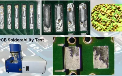
PCB Solderability Testing in Electronics Manufacturing
The PCB Solderability Test is a fundamental aspect of PCB manufacturing that ensures strong, reliable solder joints, crucial for delivering high-performance and durable products.

Peel Strength Test in PCB Manufacturing
The Peel Strength Test is a critical quality control method used to assess the adhesion strength between layers, especially in multi-layer and flexible PCBs.
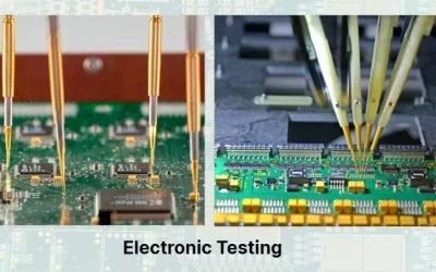
Electronic Testing in Circuit Boards and PCB Assembly
If a PCB is not thoroughly tested, issues like short circuits, open circuits, signal integrity problems, and component misplacement can lead to costly malfunctions or recalls.
Take a Quick Quote
Discover how our expertise can help with PCBA project.