
Electronic Testing in Circuit Boards and PCB Assembly

In the PCB (Printed Circuit Board) and PCBA (Printed Circuit Board Assembly) industry, Electronic Testing is an essential process that ensures boards and assembled components meet specified performance, reliability, and quality standards. As technology advances and devices become more compact and complex, the demand for rigorous electronic testing has grown significantly. In this article, we explore the critical role of electronic testing in PCB and PCBA manufacturing, the types of testing available, and the benefits of implementing a robust testing process.
Why Electronic Testing Matters in PCB & PCBA Manufacturing
Electronic testing is an integral part of PCB manufacturing and PCB assembly quality assurance, as it identifies potential issues before they reach the market. Testing helps detect problems like short circuits, open circuits, component misplacement, and signal integrity issues, all of which can compromise the functionality and reliability of the final product. For industries such as automotive, aerospace, telecommunications, and medical devices, ensuring that every PCB functions as expected is critical; any failure in these sectors could lead to costly recalls, performance issues, or safety concerns.
The goal of electronic testing is to provide manufacturers and end-users with confidence that each board will perform reliably under real-world conditions. Without thorough testing, issues like short circuits, open circuits, signal integrity problems, and component misplacement can slip through, leading to costly malfunctions or recalls. By identifying defects early, testing not only safeguards quality but also improves yield rates and production efficiency, reducing rework costs and accelerating time-to-market for new products.
Key Types of Electronic Testing in PCB & PCBA
In-Circuit Testing (ICT): In-Circuit Testing is one of the most widely implemented methods for verifying individual component values, solder joints, short circuits, and open circuits. ICT uses a bed-of-nails fixture to test each point on the board, providing fast and reliable defect detection, especially for high-volume production.
Automated Optical Inspection (AOI): AOI utilizes high-resolution cameras to inspect PCBs for visual defects, including component misplacement, soldering errors, and missing parts. By comparing each board to a reference, AOI quickly identifies surface defects without physical contact, making it ideal for rapid, non-destructive testing during assembly.
X-ray Inspection: For boards with hidden components like BGAs (Ball Grid Arrays) or complex multi-layer structures, X-ray inspection provides a view inside the board. It can detect issues such as solder voids, misaligned layers, and defects in internal connections, which are invisible to traditional AOI.
Functional Testing (FCT): Functional Testing is a final step in electronic testing where the board’s actual performance is evaluated under simulated operational conditions. It checks that the board responds correctly to expected inputs, confirming that the assembly performs all necessary functions in real-world applications.
Flying Probe Testing: Ideal for prototype and low-volume production, Flying Probe Testing does not require custom fixtures and instead uses moving probes to test each connection point on the board. This flexible method is efficient and cost-effective, especially for testing complex designs and small batches.
Burn-In Testing: Burn-In Testing involves exposing the PCB to elevated temperatures and voltages for an extended period to verify its ability to withstand long-term operational stress. Often used in critical applications like aerospace and medical devices, burn-in testing reveals potential issues related to heat and power stress before the board is deployed.
Peel Strength Test: Peel strength testing measures the adhesion strength between PCB layers, essential in multi-layer and flexible PCBs. By assessing the force required to separate layers, this test ensures that the board can withstand physical stress without delamination, especially in applications where durability is key, such as automotive and industrial environments.
Solderability Testing: Solderability testing evaluates the quality and reliability of solder joints on a PCB. This test ensures that components are securely bonded, reducing the likelihood of premature joint failure due to weak soldering. Solderability testing is particularly valuable in high-vibration or high-temperature environments where solder joint integrity is critical.
Peel Back Test: In flexible and rigid-flex PCBs, peel-back testing assesses the bond strength of the flexible material to ensure it withstands bending and twisting. This test is crucial for applications in wearable electronics, automotive, and aerospace, where durability under movement is a key requirement.
Thermal Cycling Test: Thermal cycling exposes the PCB to extreme temperature changes, verifying the board’s resilience to thermal stress and identifying potential failure points due to thermal expansion or contraction. This test is commonly used in electronics expected to endure fluctuating environmental conditions, such as outdoor or automotive devices.
Environmental Stress Screening (ESS): ESS subjects the PCB to a variety of stressors, including temperature, humidity, and vibration, to simulate real-world environmental conditions. This test is essential for identifying early failures in critical applications such as defense and telecommunications.
Insulation Resistance Testing: This test measures the resistance between isolated conductors to confirm proper insulation, preventing leakage currents that could affect circuit performance. It is particularly valuable in high-voltage applications.
Dielectric Withstanding Voltage (DWV) Testing: DWV applies a high voltage between conductors to ensure that insulation can withstand peak operating conditions without breakdown. This test is critical in ensuring long-term device safety, especially in power electronics and automotive applications.
Boundary Scan Testing (JTAG): For complex PCBs, boundary scan testing allows for testing without physical probes by using scan chains within ICs. This is highly effective in identifying connection errors and improving diagnostics in high-density PCBs.

The Benefits of Robust Electronic Testing
Enhanced Reliability and Quality: Electronic testing identifies and corrects defects that may compromise product quality, thereby enhancing overall reliability. This is particularly crucial in industries where devices must meet stringent regulatory standards and function in demanding environments.
Cost Savings and Production Efficiency: By detecting issues early in the production cycle, electronic testing reduces the cost of rework and minimizes wasted materials. It also helps prevent defective units from moving further down the production line, saving both time and money.
Improved Customer Satisfaction: Reliable testing protocols ensure that each board meets high standards, reducing the likelihood of post-sale failures. This results in fewer returns and greater customer satisfaction, which is essential for building a strong brand reputation.
Faster Time-to-Market: Effective electronic testing streamlines the production process, enabling faster turnaround times. By catching and addressing potential issues early, manufacturers can speed up the entire workflow, reducing delays and accelerating product launches.
Choosing the Right Electronic Testing Method
Selecting the appropriate testing method depends on various factors, including production volume, board complexity, and application requirements. For instance, In-Circuit Testing and Automated Optical Inspection are ideal for high-volume production, while Flying Probe Testing is suited for prototypes or low-volume runs. High-complexity boards, such as those used in telecommunications and medical devices, often benefit from X-ray Inspection and Burn-In Testing to verify performance under stress.
Additionally, many manufacturers implement a combination of testing methods for comprehensive coverage. For example, AOI may be used for initial defect detection, followed by ICT or functional testing to confirm circuit integrity and functionality. Combining testing methods ensures that all aspects of the board are evaluated, from basic functionality to stress resilience.
Questions to Ask PCB Factories about Testing Services
When evaluating potential PCB factories, ask the following questions to understand their testing capabilities and how they align with your needs:
- What electronic testing methods do you offer, and at what stages in the production process are they applied?
- Are your testing methods tailored for specific applications or industries, like automotive, medical, or consumer electronics?
- Can you provide reports and certifications for each test performed, especially for compliance with industry standards?
- Do you offer customized functional testing to replicate real-world conditions specific to my product?
- What measures do you have in place for quality control if defects are detected during testing?
- Is thermal cycling or burn-in testing available for high-stress applications?
- How frequently is Automated Optical Inspection (AOI) used in the production line, and do you use 3D AOI for better accuracy?
- If I have low-volume or prototype requirements, do you provide flying probe testing or other suitable options?
Asking these questions helps you determine whether the factory’s testing protocols meet the reliability and performance standards necessary for your project.

Benefits of Partnering with a Factory that Provides Comprehensive Electronic Testing
Partnering with a PCB manufacturer that emphasizes comprehensive electronic testing significantly enhances product reliability. With rigorous testing protocols, manufacturers can identify and address potential defects early in the production process, reducing the chance that faulty products reach the market. This ensures that each PCB operates as intended, meeting the high-quality standards expected, particularly in critical applications such as automotive, aerospace, and medical devices.
Effective testing also leads to cost savings by detecting issues before they progress further down the production line. Early identification of defects lowers rework costs, minimizes waste, and makes the entire process more cost-effective. These savings benefit not only the manufacturer but also the client, as they allow for a smoother production cycle with fewer disruptions, creating a more efficient path from design to finished product.
Moreover, comprehensive testing builds customer satisfaction and trust by reducing the likelihood of field failures and returns. When a product performs reliably, customers are more likely to have a positive experience, leading to improved brand loyalty and reputation. By choosing a testing-focused manufacturer, companies can confidently bring high-quality products to market more quickly, supporting brand integrity and competitive advantage.
In the PCB & PCBA industry, Electronic Testing is indispensable for ensuring the quality, reliability, and safety of electronic devices. By implementing rigorous testing protocols, manufacturers can detect potential issues early, optimize production efficiency, and deliver high-quality products to market. As technology advances and boards become increasingly complex, electronic testing will continue to evolve, incorporating more sophisticated methods to address emerging challenges in electronics manufacturing.
For companies aiming to produce reliable, high-performance PCBs, investing in a robust electronic testing process is essential. Whether through ICT, AOI, or advanced methods like X-ray inspection, the right testing approach not only enhances product quality but also supports operational efficiency, customer satisfaction, and brand reputation in a competitive market.
Get a Free PCB & PCBA Quote

Recommended Posts
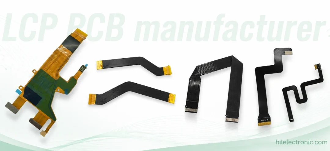
LCP PCB Manufacturer for High-Frequency and Compact Electronic Products
The phrase “LCP PCB manufacturer” covers several very...
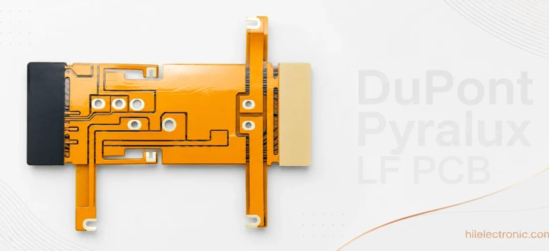
DuPont Pyralux LF PCB Manufacturing for Flexible Circuit Projects
A Pyralux LF flex circuit should be quoted from its...
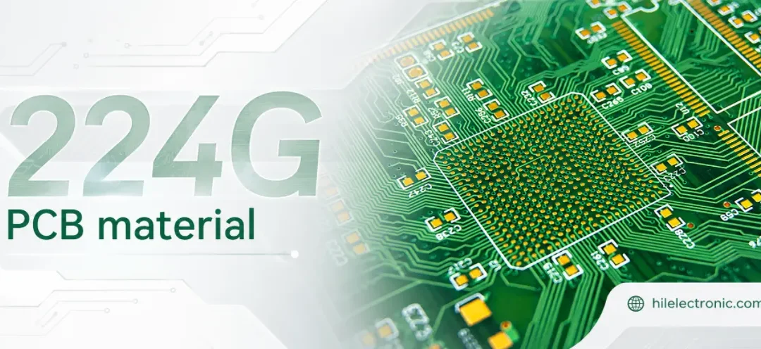
224G PCB Material Selection for Manufacturable PAM4 Channels
A 224G PCB request becomes actionable only when the...
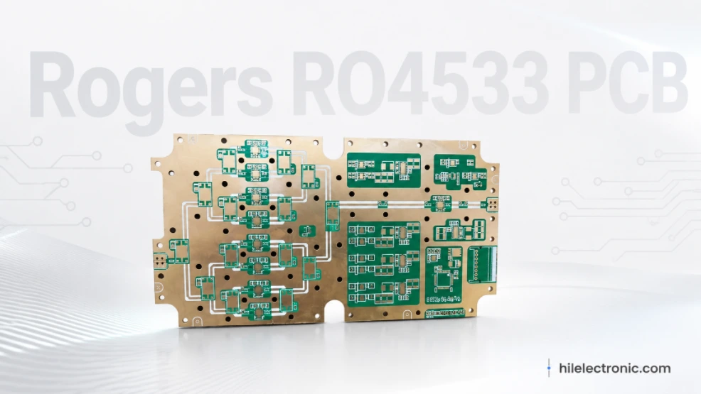
Rogers RO4533 PCB Manufacturing for Cost-Sensitive RF Products
RO4533 should be handled as a grade-specific commercial RF...
How to get a quote for PCBs
Let us run DFM/DFA analysis for you and get back to you with a report.
You can upload your files securely through our website.
We require the following information in order to give you a quote:
-
- Gerber, ODB++, or .pcb, spec.
- BOM list if you require assembly
- Quantity
- Turn time
In addition to PCB manufacturing, we offer a comprehensive range of electronic services, including PCB design, PCBA (Printed Circuit Board Assembly), and turnkey solutions. Whether you need help with prototyping, design verification, component sourcing, or mass production, we provide end-to-end support to ensure your project’s success. For PCBA services, please provide your BOM (Bill of Materials) and any specific assembly instructions. We also offer DFM/DFA analysis to optimize your designs for manufacturability and assembly, ensuring a smooth production process.