
The Comprehensive Guide to Electronic Packaging: Electronic Manufacturing in China

What is Electronic Packaging?
Electronic packaging refers to the process of enclosing, supporting, and protecting electronic components, circuits, and modules within a protective housing or enclosure. This packaging serves multiple essential functions: it provides mechanical support, shields delicate electronics from environmental factors like moisture and dust, blocks electromagnetic interference (EMI), and facilitates thermal management by dissipating heat generated by active components. Additionally, electronic packaging includes interconnections and interfaces that enable reliable integration with other systems and ensure signal integrity.
Electronic packaging is a critical aspect of electronics manufacturing, affecting the durability, reliability, performance, and efficiency of electronic devices in diverse applications, from consumer electronics to industrial equipment and high-performance computing systems. Effective packaging ensures that electronic components can withstand operational stresses, perform consistently, and maintain a long service life.
Why is Electronic Packaging Important?
Electronic packaging is not merely an outer shell; it plays a vital role in ensuring device functionality, safety, and longevity. Here’s why effective electronic packaging is indispensable:
- Physical Protection: Packaging protects delicate components from physical impacts, vibrations, and shock, which is critical in ruggedized or portable devices.
- Environmental Shielding: High-quality packaging prevents exposure to moisture, contaminants, and dust that could lead to corrosion or short circuits, especially in harsh environments.
- Electromagnetic Interference (EMI) Shielding: Packaging blocks interference from external electromagnetic fields and mitigates cross-talk between internal signals, ensuring signal fidelity.
- Thermal Management: Packaging materials with high thermal conductivity facilitate heat dissipation, preventing overheating and thermal runaway in high-power applications.
- Structural Integrity and Reliability: Proper packaging provides mechanical stability and vibration dampening, ensuring reliable operation even under variable thermal and mechanical conditions.
In summary, electronic packaging is crucial for maintaining signal integrity, thermal stability, structural integrity, and environmental protection, making it an integral part of the design and manufacturing of high-performance electronic devices.
Types of Electronic Packaging Materials
Various materials are used in electronic packaging, each selected for its specific properties to address challenges such as heat dissipation, electrical insulation, mechanical support, and chemical resistance.
- Plastic Resins: Commonly used in consumer electronics, materials like epoxy resin, phenolic, and silicone resin offer excellent electrical insulation and can be molded into complex shapes, providing a protective housing.
- Ceramics: Ceramics like alumina (Al₂O₃), aluminum nitride (AlN), and silicon carbide (SiC) are ideal for high-performance applications due to their thermal conductivity, electrical insulation, and chemical stability.
- Metals: Metals such as aluminum, copper, and gold are known for superior thermal and electrical conductivity. Aluminum is used for heat sinks, while copper and gold are preferred for interconnects due to their low resistance and high conductivity.
- Composite Materials: Composites combine the strengths of multiple materials, such as polymer-fiber composites that enhance mechanical strength, thermal management, and durability.
- Thermal Interface Materials (TIMs): TIMs, like thermal grease, phase-change materials, and thermal pads, facilitate efficient heat transfer between components and heat sinks, which is critical in high-power and high-frequency applications.
- Adhesives and Encapsulants: Adhesives such as polyurethane and silicone encapsulants protect against moisture, contaminants, and vibrations, providing conformal coating and securing components in place.
Each material is chosen based on its thermal, electrical, and mechanical properties, which ultimately affect the efficiency, reliability, and safety of the electronic device.

Key Considerations in Selecting Electronic Packaging Materials
Selecting the appropriate materials for electronic packaging is fundamental to achieving optimal performance, reliability, and durability, especially in applications where failure is not an option. A key factor to consider is thermal conductivity, as materials with high thermal conductivity are essential for dissipating heat from high-power components, preventing thermal degradation, and maintaining thermal equilibrium. Thermal expansion is also critical; matching the thermal expansion coefficients of the packaging materials with those of components, like silicon chips, minimizes thermal stress and prevents issues like cracking or delamination, which could compromise the device’s structural integrity.
Electrical insulation is another essential criterion in material selection. High dielectric strength materials prevent short circuits and ensure electrical isolation between components, which is vital for maintaining signal integrity and preventing device malfunction. In addition, materials used in electronic packaging must have sufficient mechanical strength and toughness to withstand physical stress, such as shocks and vibrations, encountered during operation, transportation, and handling. This strength ensures that the electronic assembly remains operational and intact throughout its lifecycle, even in demanding conditions.
Furthermore, moisture resistance and chemical stability are crucial for applications in humid or chemically active environments, where exposure to moisture and corrosive substances could lead to corrosion or degradation. Finally, cost-effectiveness is an important consideration for large-scale manufacturing; materials should offer the best balance between performance and affordability, allowing manufacturers to maintain quality without excessive costs. By evaluating materials based on these criteria, manufacturers can ensure that the selected packaging solutions support both functional and economic goals for efficient mass production and long-term reliability in high-performance electronics.
Types of Electronic Packaging Methods
Electronic packaging encompasses a variety of methods, each chosen based on factors like component density, signal integrity, and thermal management:
Through-Hole Technology (THT): Components with leads are inserted into PCB holes and soldered on the opposite side. THT offers strong mechanical bonds and is suitable for components subjected to physical stress but occupies more space.
Surface-Mount Technology (SMT): Components are mounted directly onto the PCB surface, allowing for higher component density and smaller board sizes. SMT is prevalent in compact consumer devices.
Chip-on-Board (COB): Semiconductor chips are directly mounted onto a PCB and encapsulated, enhancing heat dissipation and electrical performance by reducing the distance between chip and connections.
Ball Grid Array (BGA): A grid of solder balls on the underside of the component creates electrical connections with the PCB. BGA packaging is ideal for high-speed and high-frequency circuits due to excellent signal integrity and thermal efficiency.
System-in-Package (SiP): Multiple components, such as processors, memory, and sensors, are integrated into a single package, ideal for compact designs in mobile devices and IoT applications.
Chip Scale Package (CSP): A miniaturized version of BGA where the package closely matches the chip size, reducing footprint and enhancing thermal dissipation in portable electronics.
Package-on-Package (PoP): Stacks multiple packages vertically, enabling the integration of memory and processing units in a compact form factor, often used in mobile and high-density applications.
Each packaging method is selected based on factors like performance requirements, thermal constraints, signal integrity, and cost.

Advanced Electronic Packaging Technologies
With increasing device complexity, electronic packaging has evolved to incorporate advanced technologies to meet rigorous performance standards. Some cutting-edge packaging technologies include:
High-Temperature Co-Fired Ceramics (HTCC): Multilayer ceramic substrates used in high-temperature and high-power applications for enhanced durability and performance.
Low-Temperature Co-Fired Ceramics (LTCC): Ideal for multilayer circuits in compact, high-frequency applications where precision is crucial.
Direct Bonded Copper (DBC): Utilizes copper bonded to ceramic substrates for excellent thermal conductivity in power electronics.
Laser Activated Metal Ceramics (LAM): Supports high-frequency applications by combining ceramic properties with metal precision, used in high-performance RF systems.
These technologies enable improved thermal performance, miniaturization, and durability, supporting applications that require high reliability under demanding conditions.
Key Challenges in Electronic Packaging and How to Address Them for Reliable, High-Performance Devices
As electronic devices become more powerful and compact, electronic packaging faces critical challenges that demand innovative solutions to ensure reliable performance, longevity, and safety. One of the most pressing issues is thermal management. With increased power densities, components produce substantial heat that, if not effectively dissipated, can lead to thermal degradation and even device failure. To address this, advanced cooling solutions such as heat pipes, thermal interface materials (TIMs), and micro-channel cooling are essential, particularly in high-power applications like telecommunications and automotive electronics. Implementing these strategies helps maintain safe operating temperatures, thereby enhancing the performance and lifespan of devices.
Miniaturization is another significant challenge, as the demand for smaller, more compact devices continues to grow. Achieving this requires advanced 3D packaging techniques and high-density interconnects (HDIs), which allow manufacturers to maximize functionality within a limited space. Effective miniaturization not only saves space but also allows for increased portability without sacrificing performance. Additionally, mechanical reliability is vital—packaging materials must withstand physical stresses such as vibrations, impacts, and thermal cycling without cracking or delaminating, particularly in portable or rugged environments. Ensuring environmental protection is also crucial, as effective barriers against moisture, dust, and contaminants are essential for safeguarding components, especially in harsh operating conditions. Lastly, material compatibility remains a core requirement, as packaging materials must align with the thermal and mechanical properties of internal components to prevent thermal mismatch and ensure long-term stability. By prioritizing advancements in materials science, engineering, and process optimization, manufacturers can effectively address these challenges, ultimately creating electronic devices that are more reliable, durable, and capable of meeting today’s complex demands.
Understanding and addressing the challenges in electronic packaging is crucial for manufacturers aiming to produce high-performance, long-lasting devices. By focusing on thermal management, miniaturization, mechanical reliability, environmental protection, and material compatibility, companies can create packaging solutions that enhance device functionality and durability. These insights provide valuable guidance for engineers and manufacturers committed to advancing the reliability and efficiency of modern electronics.
At Highleap Electronic, we are committed to providing cutting-edge electronic packaging solutions that meet the evolving needs of modern electronics. Our expertise spans from high-density PCB design and manufacturing to advanced packaging solutions that ensure reliability, durability, and performance. Whether you need custom packaging materials, thermal management solutions, or full turnkey packaging services, Highleap Electronic has the resources and expertise to support your project.
Contact us today to discuss how our electronic packaging services can enhance the functionality, longevity, and quality of your next electronic product. With Highleap Electronic, you get a trusted partner dedicated to excellence in every aspect of electronic packaging.
Get a Free PCB & PCBA Quote

Recommended Posts
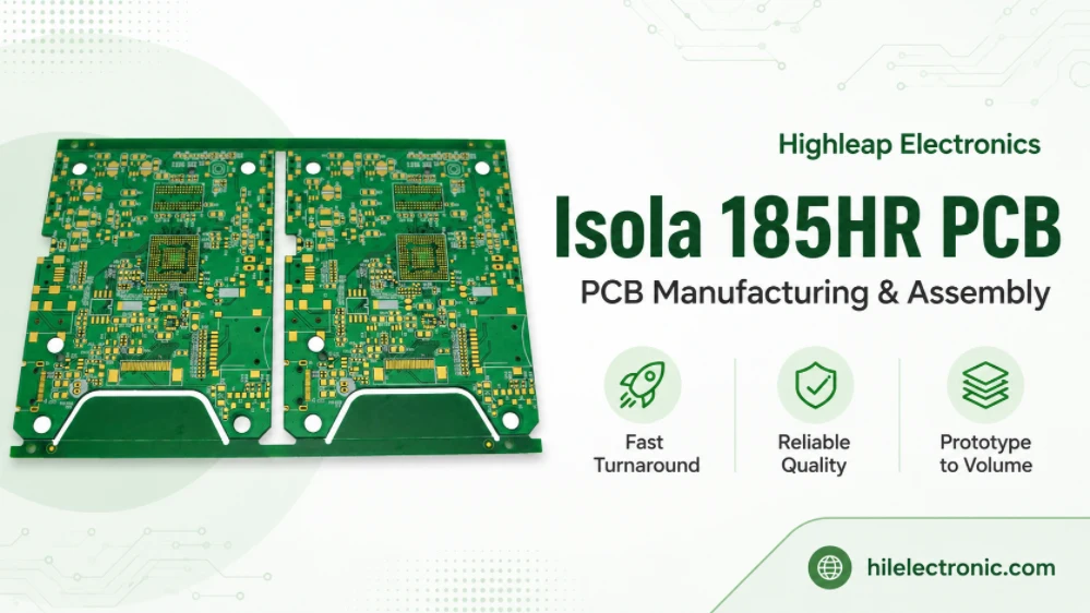
Isola 185HR PCB Manufacturer for High-Reliability Multilayers
Isola 185HR belongs on a manufacturing page about...
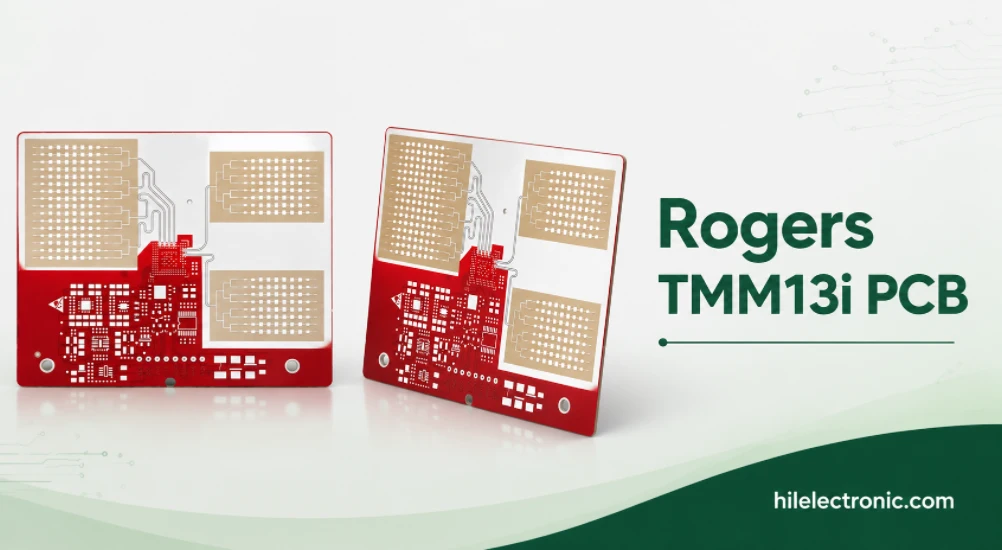
Rogers TMM13i PCB Manufacturer for Ultra-Miniature RF Substrates
TMM13i is used when a microwave circuit must become very...
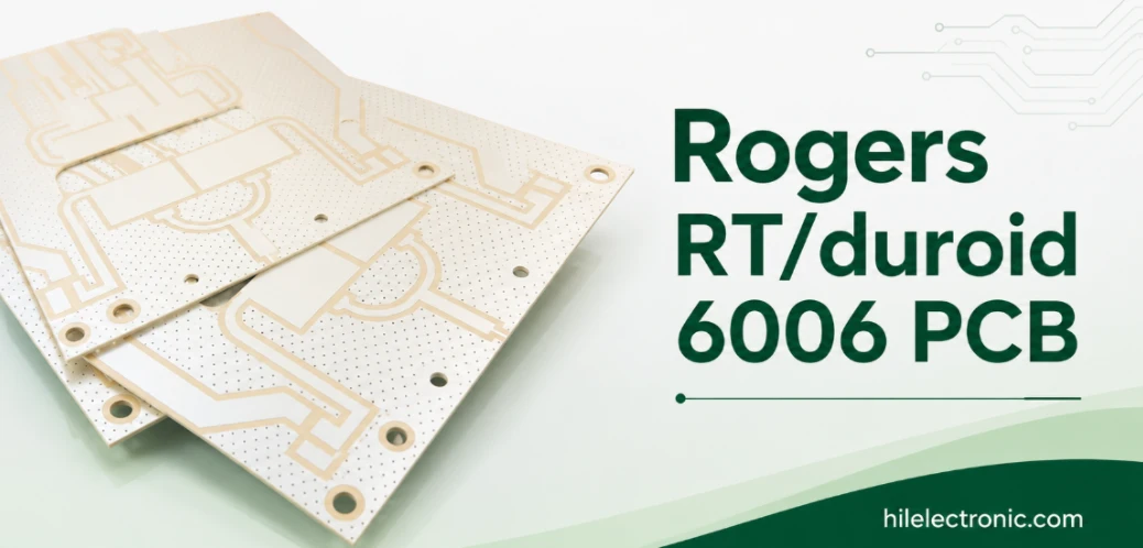
RT/duroid 6006 PCB Manufacturer for Compact High-Dk Microwave Circuits
RT/duroid 6006 is selected when circuit area is expensive....
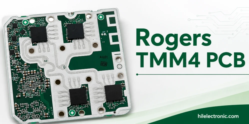
Rogers TMM4 PCB Manufacturer for Compact Microwave Filters
TMM4 is most useful when a microwave circuit must become...
How to get a quote for PCBs
Let us run DFM/DFA analysis for you and get back to you with a report.
You can upload your files securely through our website.
We require the following information in order to give you a quote:
-
- Gerber, ODB++, or .pcb, spec.
- BOM list if you require assembly
- Quantity
- Turn time
In addition to PCB manufacturing, we offer a comprehensive range of electronic services, including PCB design, PCBA (Printed Circuit Board Assembly), and turnkey solutions. Whether you need help with prototyping, design verification, component sourcing, or mass production, we provide end-to-end support to ensure your project’s success. For PCBA services, please provide your BOM (Bill of Materials) and any specific assembly instructions. We also offer DFM/DFA analysis to optimize your designs for manufacturability and assembly, ensuring a smooth production process.