
Thermal Simulation in MCPCB Design: How to Predict Hot Spots

Why MCPCB Thermal Simulation is Critical in Design
Metal Core Printed Circuit Boards serve critical roles in high-power LED systems, automotive lighting, and power modules where thermal management determines product reliability. These applications generate substantial heat that must be efficiently dissipated to prevent component failure and performance degradation.
Even when designers select high thermal conductivity materials, improper component placement or inadequate thermal path design can create localized hot spots that compromise system integrity. Traditional experience-based design approaches often fail to predict these thermal bottlenecks until physical prototypes reveal problems.
MCPCB thermal simulation enables engineers to predict and mitigate hot spots before fabrication, providing quantitative temperature distribution data that transforms thermal design from guesswork into precision engineering. This proactive approach identifies thermal issues during the design phase when modifications cost significantly less than post-fabrication corrections.
How MCPCB Thermal Simulation Transforms Heat Transfer Analysis
Thermal simulation evaluates heat dissipation performance by analyzing conduction paths, interface thermal resistance, and component temperature rise within the MCPCB structure. Unlike empirical design methods that rely on rough calculations and past experience, simulation provides detailed spatial temperature mapping.
The primary objective focuses on reducing junction temperature while optimizing copper layer routing for balanced heat distribution. Engineers can test multiple design iterations virtually, comparing thermal performance across different material selections and component arrangements without manufacturing physical samples.
This analytical capability distinguishes modern MCPCB thermal simulation from conventional approaches. Simulation quantifies the thermal impact of each design decision, allowing engineers to make informed tradeoffs between thermal performance, manufacturing cost, and design complexity.
Critical Simulation Outputs
Temperature distribution maps reveal hot spot locations and thermal gradient severity across the board surface. Heat flux vectors show the direction and magnitude of thermal energy flow through each layer. Junction temperature predictions for individual components indicate whether designs meet manufacturer specifications and reliability targets.
Thermal Modeling Fundamentals for MCPCB Structures
The layered architecture of MCPCBs presents unique modeling challenges in thermal simulation. Heat flows through a series of interfaces starting from the copper circuit layer, passing through the dielectric insulation layer, continuing into the metal base plate, and finally transferring to external heat sinks.
Each layer’s thermal conductivity directly influences overall heat transfer efficiency, with the dielectric insulation layer typically presenting the highest thermal resistance in the stack-up. Small variations in insulation thickness or material properties produce significant temperature differences.
Thermal modeling requires precise input of thermal conductivity values for copper traces, aluminum or copper base plates, and specialized dielectric materials. The simulation solves steady-state or transient heat transfer equations using these material properties combined with geometric dimensions.
Material Property Sensitivity in MCPCB Thermal Simulation
Dielectric layer thickness variations of even 25 micrometers can alter junction temperatures by several degrees Celsius. Base plate material selection between aluminum and copper changes thermal resistance by factors of two or more. These sensitivities underscore why accurate material data proves essential for reliable simulation results rather than nominal handbook values.

MCPCB Heat Dissipation
MCPCB Thermal Simulation Workflow: From Model to Results
The simulation process follows a systematic sequence that transforms design concepts into predictive thermal analysis. Engineers begin by defining geometry, creating a three-dimensional representation of the MCPCB layer stack-up including copper trace patterns, dielectric thickness, and base plate dimensions.
Material property assignment follows geometry definition, specifying thermal conductivity for each layer along with specific heat capacity and density if transient analysis is required. Accurate material data proves critical since MCPCB thermal simulation results depend entirely on these input parameters.
Five Essential Steps in Thermal Simulation
The workflow progresses through distinct phases that build comprehensive thermal models:
- Define geometry – Input layer stack-up structure and dimensional specifications for all MCPCB components
- Assign material properties – Specify thermal conductivity, density, and specific heat for copper, dielectric, and base layers
- Set power sources and boundary conditions – Apply component power dissipation values and define thermal interfaces with heat sinks
- Run finite element analysis – Execute simulation using tools such as ANSYS, COMSOL Multiphysics, or SolidWorks Flow Simulation
- Interpret thermal results – Analyze temperature contour plots to identify maximum temperatures and problematic hot spot locations
Solution convergence requires appropriate mesh refinement, particularly in regions with steep temperature gradients near high-power components. Result interpretation examines whether predicted junction temperatures remain within component specifications and assesses thermal margin available for design variations.
Identifying Hot Spots Through MCPCB Thermal Simulation Results
Temperature distribution visualization uses color-coded thermal maps where red zones indicate areas exceeding target temperatures. Hot spot identification focuses attention on regions requiring design modifications, whether through component relocation, enhanced copper coverage, or improved thermal interface materials.
Optimization strategies emerge directly from simulation insights. Moving components away from thermal bottlenecks, increasing copper thickness in high-heat-flux areas, or redesigning trace routing to spread heat more uniformly all represent responses to simulation-identified issues.
Iterative Design Refinement
MCPCB thermal simulation supports an iterative optimization cycle where engineers modify designs based on thermal analysis, re-simulate to verify improvements, and continue refining until temperature targets are achieved. This simulation-driven iteration occurs entirely in the digital domain.
Interface thermal resistance reduction through improved thermal interface materials or bonding processes often provides significant temperature reductions when simulation shows high resistance at layer boundaries. Non-uniform power distribution across multiple components creates avoidable hot spots that layout changes can eliminate.
Common MCPCB Thermal Simulation Pitfalls and Best Practices
Many thermal simulations underestimate interface thermal resistance between MCPCB layers and external heat sinks, producing overly optimistic temperature predictions. Including realistic contact resistance values, often derived from manufacturer specifications or experimental measurements, significantly improves simulation accuracy.
Using inaccurate thermal conductivity data represents another frequent error. Generic material properties from databases may not match the specific materials and processing conditions in production MCPCBs. Obtaining validated thermal property data from material suppliers enhances simulation reliability.
Critical Factors Often Overlooked
Engineers should address these common modeling gaps to ensure accurate MCPCB thermal simulation results:
- Interface thermal resistance – Contact resistance between layers and heat sink interfaces often contributes 20-40% of total thermal resistance
- Non-uniform power density – Semiconductor devices concentrate heat generation in small die areas rather than distributing uniformly across packages
- Solder layer thermal impact – Thermal interface material thickness and conductivity significantly affect heat transfer paths between components and copper
Power density assumptions must reflect actual component behavior rather than simplified uniform dissipation models. Many semiconductor devices require detailed modeling of component internal thermal resistance for accurate junction temperature prediction.
Simulation validation through experimental testing remains essential for establishing confidence in predictions. Thermal measurements on prototype boards using thermocouples or infrared cameras verify MCPCB thermal simulation accuracy and identify any modeling assumptions requiring refinement.
Enhancing MCPCB Design Reliability Through Thermal Simulation
Effective MCPCB thermal simulation transforms heat management from reactive troubleshooting into proactive performance optimization. By identifying hot spots and optimizing heat transfer paths before production, engineers can significantly reduce development cycles, prevent overheating issues, and improve long-term system reliability.
At Highleap Electronics, we integrate thermal simulation into every stage of MCPCB design and manufacturing to ensure consistent thermal performance and quality results. Our strengths include:
-
Comprehensive thermal modeling – Advanced simulation tools to predict temperature distribution and identify critical thermal bottlenecks.
-
Material and structure optimization – Engineering-driven selection of dielectric materials, copper thickness, and base metals to achieve optimal thermal balance.
-
Design-to-production integration – Seamless transition from virtual analysis to manufacturing, ensuring simulation results align with real-world performance.
-
High-reliability manufacturing – ISO9001, ISO13485, ISO14001, and IATF16949 certified production processes that guarantee quality and consistency across every build.
Contact Highleap Electronics to learn how our simulation-driven approach can enhance your next MCPCB project. We help you transform thermal challenges into reliable, production-ready solutions.

Recommended Posts

Electronic Contract Assembly: Models, Selection, and the Full Build Process
Figure 1. Electronic Contract Assembly reference image for...

How to Clean Flux Off a PCB: The Right Method for Each Flux Type
Figure 1. How To Clean Flux Off Pcb reference image for...
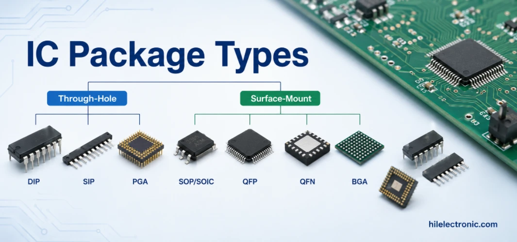
IC Package Types Explained: BGA vs QFN vs QFP, and How to Choose for Your PCB
Figure 1. IC package types image for PCB manufacturing...

Copper Clad Boards (Copper-Clad Laminate): What They Are, Types, and How PCBs Are Made From Them
Figure 1. copper clad boards image for PCB manufacturing...
How to get a quote for PCBs
Let‘s run DFM/DFA analysis for you and get back to you with a report. You can upload your files securely through our website. We require the following information in order to give you a quote:
-
- Gerber, ODB++, or .pcb, spec.
- BOM list if you require assembly
- Quantity
- Turn time
In addition to PCB manufacturing, we offer a comprehensive range of electronic services, including PCB design, PCBA, and turnkey solutions. Whether you need help with prototyping, design verification, component sourcing, or mass production, we provide end-to-end support to ensure your project’s success.
For PCBA services, please provide your BOM (Bill of Materials) and any specific assembly instructions. We also offer DFM/DFA analysis to optimize your designs for manufacturability and assembly, ensuring a smooth production process.