
Metal Core PCB Design Guidelines | Engineering Guidelines for Optimal Thermal Performance

Introduction
Metal core PCB design represents a critical engineering discipline for applications demanding superior thermal management capabilities. As power densities continue to increase in LED lighting systems, automotive electronics, and power conversion modules, the design phase has emerged as the primary determinant of thermal performance rather than material selection alone.
This guide focuses on the engineering parameters that define successful Metal core PCB design, including layout strategies, heat path optimization, copper thickness specifications, and thermal via implementation. Effective thermal management PCB design requires systematic consideration of these interconnected factors from the initial concept stage through manufacturing validation.
Understanding the Design Objective in Metal Core PCB Design
The fundamental objective of Metal Core PCB design extends beyond simple heat conduction to achieve uniform thermal distribution while maintaining long-term reliability. The three-layer structure comprising copper circuit layer, thermally conductive dielectric, and metal base substrate imposes specific design constraints that must be addressed early in the development cycle.
Design engineers must evaluate heat source positioning, copper weight requirements, and mechanical mounting interfaces during initial planning. The metal base acts as both a heat spreader and structural element, necessitating careful consideration of thermal expansion coefficients and attachment methods to external heat sinks.

Metal Core PCB Stackup
Layout Design Guidelines for Thermal Optimization
Component placement strategy forms the foundation of effective Metal Core PCB design. High thermal density components should be positioned along the primary heat dissipation path, typically centered over mounting points that connect to external cooling systems. Even distribution of heat-generating devices prevents localized hot spots that can compromise component reliability and accelerate system degradation.
Strategic Component Placement
Thermal simulation tools provide invaluable insight during the layout phase, allowing engineers to visualize heat flow patterns and identify potential thermal bottlenecks before committing to fabrication. Circuit trace width and copper foil thickness directly influence lateral heat spreading within the copper layer. Wider traces adjacent to power components facilitate thermal distribution while simultaneously supporting higher current capacity.
Heat Source Distribution Analysis
Design teams should map the thermal profile of the entire assembly, accounting for both steady-state operation and transient thermal events. Adjacent components must be spaced with consideration for thermal coupling effects and the combined thermal load on the metal base substrate.
Via and Thermal Path Design
Thermal vias serve a specialized function in Metal Core PCB design by creating vertical heat conduction paths through the dielectric layer to the metal base. Although most metal core boards utilize single-sided copper circuitry, strategic placement of filled thermal vias beneath high-power components significantly reduces thermal resistance. An array pattern of thermal vias provides multiple parallel heat paths, effectively lowering the overall thermal impedance.
Recommended Via Specifications
Engineering experience suggests thermal via diameters between 0.3 and 0.5 millimeters with center-to-center spacing of 1.0 to 1.5 millimeters for optimal performance. Copper plating thickness of 35 to 70 micrometers ensures adequate heat conduction while maintaining manufacturing feasibility. The via pattern density should be maximized within the thermal pad area beneath power devices, with consideration given to the mechanical integrity of the dielectric layer.
Copper Thickness Selection and Trace Design
Copper weight specification represents a critical design decision in Metal Core PCB design that affects both thermal and electrical performance. Standard LED and consumer electronics applications typically employ one-ounce copper (35 micrometers), providing adequate current capacity and heat spreading for moderate power levels. Power electronics modules operating at elevated current densities require two to three-ounce copper (70 to 105 micrometers) to prevent excessive resistive heating and enable effective lateral heat distribution.
Balancing Performance and Manufacturability
Heavier copper improves current carrying capacity and thermal conductance but introduces challenges in photolithography and etching processes, potentially limiting minimum trace width and spacing. Selective copper plating in high-current zones offers a compromise approach, maintaining fine-pitch capability in signal areas while reinforcing power distribution networks. Design engineers must collaborate with manufacturing partners to verify copper thickness selections align with production capabilities and tolerance requirements.

LED Metal Core PCB
Dielectric Layer Considerations
The thermally conductive dielectric layer functions as the primary thermal bottleneck in Metal Core PCB design, and its properties fundamentally determine overall thermal resistance. Thinner dielectric layers with higher thermal conductivity values reduce thermal impedance, though electrical insulation requirements and voltage withstand specifications impose practical limits. Typical dielectric thermal conductivity ranges from 1 to 3 watts per meter-kelvin, with thickness values between 50 and 150 micrometers.
Engineers must balance competing requirements of low thermal resistance, high dielectric strength, and long-term reliability under thermal cycling conditions. MCPCB Material selection involves tradeoffs between thermal performance and electrical isolation, particularly in high-voltage applications where increased dielectric thickness becomes necessary for safety compliance.
Thermal Simulation and Validation
Computational thermal analysis should be integrated into the Metal Core PCB design workflow to validate heat dissipation strategies before prototype fabrication. Software tools such as ANSYS or similar finite element analysis platforms enable designers to model complex thermal interactions and predict junction temperatures under various operating conditions. Key performance metrics include thermal resistance from junction to case and anticipated temperature rise above ambient conditions.
Validation Testing Protocols
Physical validation using infrared thermal imaging confirms simulation predictions and identifies unexpected hot spots in prototype assemblies. Power cycling tests evaluate thermal performance under realistic operating profiles and assess long-term reliability through accelerated aging protocols. Correlation between simulated and measured results builds confidence in the thermal design methodology and guides refinement for subsequent design iterations.
Manufacturing Design Considerations
Design for manufacturability principles apply equally to Metal Core PCB design as to conventional printed circuits, though metal core boards present unique processing constraints. Extremely thick copper specifications, dense thermal via patterns, and tight dimensional tolerances can significantly impact manufacturing yield and production costs. Early engagement with fabrication partners ensures design features align with process capabilities.
Process Compatibility Factors
Copper etching precision, dielectric layer lamination tolerances, and surface finish compatibility all require verification during design reviews. Conventional surface treatments including organic solderability preservative and electroless nickel immersion gold remain compatible with metal core substrates, though process parameters may require adjustment. Manufacturing documentation should clearly specify critical dimensions, material requirements, and inspection criteria to ensure consistent production quality.
Conclusion
Effective Metal Core PCB design requires a systematic and engineering-driven approach to thermal management. Each design parameter—layout configuration, copper thickness, thermal via design, and dielectric selection—contributes interactively to the board’s overall thermal efficiency and long-term reliability. Achieving optimal performance depends on balancing these factors within real manufacturing constraints.
At Highleap Electronics, we combine design expertise and precision manufacturing to deliver reliable Metal Core PCB solutions for demanding applications. Our capabilities include:
- Engineering Design Support – Thermal path optimization, copper thickness evaluation, and layout review tailored to high-power applications.
- Advanced Manufacturing Control – Precise copper etching, thermal via drilling, and consistent dielectric lamination for optimal heat dissipation.
- Quality and Reliability Assurance – ISO9001, ISO13485, ISO14001, and IATF16949 certified production ensuring consistent performance and traceability.
By integrating PCB design and PCB manufacturing expertise, Highleap Electronics helps customers achieve efficient, cost-effective, and scalable Metal Core PCB solutions that meet the highest thermal management standards. Contact our engineering team today to discuss your Metal Core PCB design requirements and optimize your next high-power electronic project.

Recommended Posts
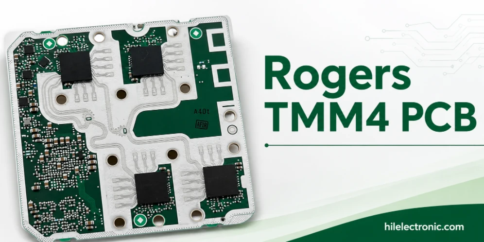
Rogers TMM4 PCB Manufacturer for Compact Microwave Filters
TMM4 is most useful when a microwave circuit must become...
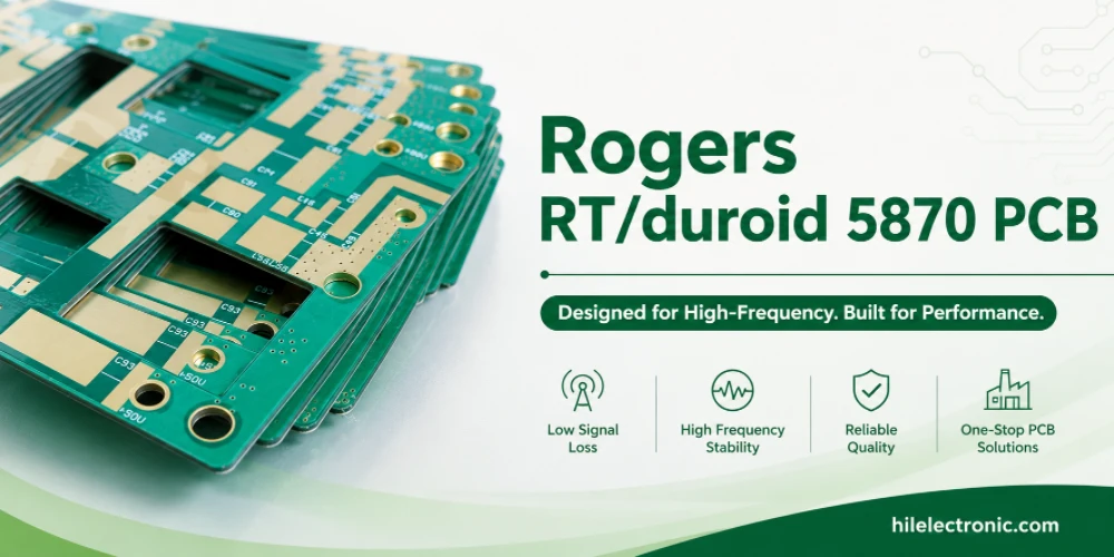
RT/duroid 5870 PCB Manufacturer for Low-Loss PTFE RF Circuits
RT/duroid 5870 is chosen when the RF path needs low loss,...
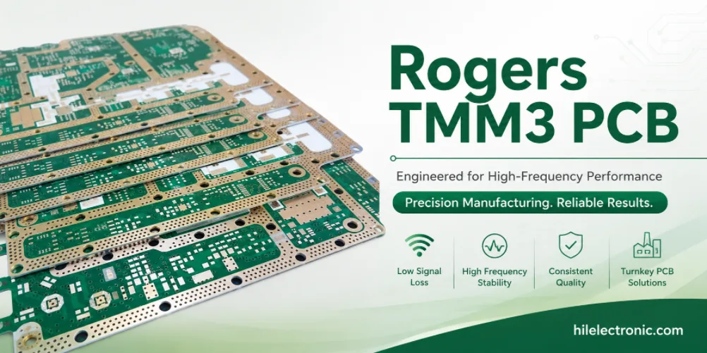
Rogers TMM3 PCB Manufacturer for Mechanical RF Modules
TMM3 is selected when an RF circuit must behave as part of...
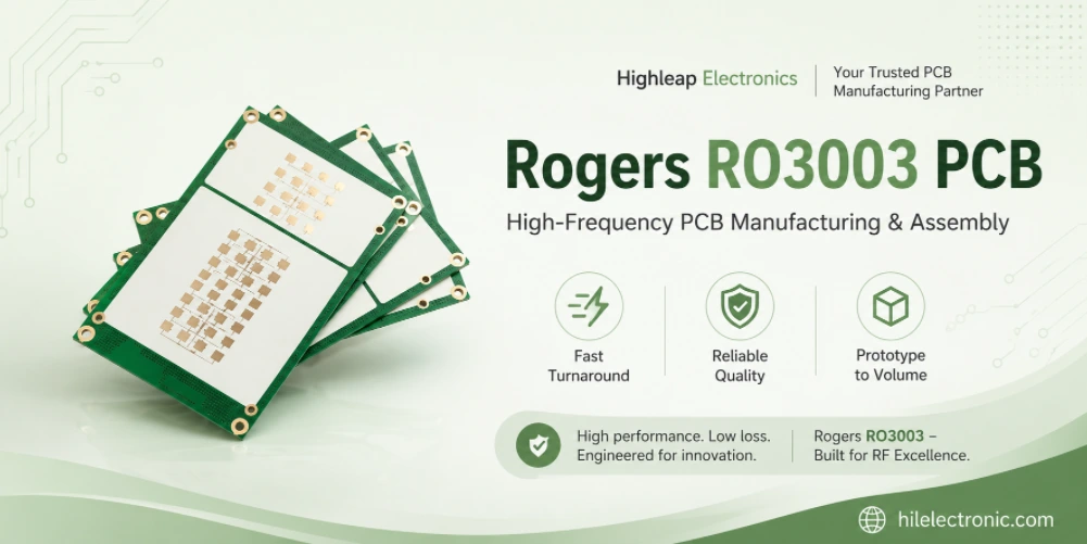
Rogers RO3003 PCB Manufacturer for Automotive Radar and mmWave Modules
A 77 GHz radar board is purchased as a working sensor...
How to get a quote for PCBs
Let‘s run DFM/DFA analysis for you and get back to you with a report. You can upload your files securely through our website. We require the following information in order to give you a quote:
-
- Gerber, ODB++, or .pcb, spec.
- BOM list if you require assembly
- Quantity
- Turn time
In addition to PCB manufacturing, we offer a comprehensive range of electronic services, including PCB design, PCBA, and turnkey solutions. Whether you need help with prototyping, design verification, component sourcing, or mass production, we provide end-to-end support to ensure your project’s success.
For PCBA services, please provide your BOM (Bill of Materials) and any specific assembly instructions. We also offer DFM/DFA analysis to optimize your designs for manufacturability and assembly, ensuring a smooth production process.