
HDI PCB Design Guidelines: Engineering Excellence in High-Density Interconnect Technology

Introduction
High-Density Interconnect PCB technology represents a fundamental shift in printed circuit board design methodology, enabling unprecedented component density and electrical performance in modern electronic devices. As consumer electronics, automotive systems, and industrial applications demand smaller form factors with enhanced functionality, HDI PCB design has become an essential competency for engineers developing competitive products.
The integration of microvias, sequential lamination processes, and advanced materials allows designers to achieve routing densities that were previously impossible with conventional PCB manufacturing techniques. This guide examines the critical design principles and manufacturing considerations that define successful HDI PCB implementation.
Understanding HDI PCB Fundamentals
Core Characteristics of HDI Technology
HDI PCB design distinguishes itself through several defining features that directly impact circuit density and performance. Microvias with diameters typically ranging from 0.004 inches to 0.006 inches enable connections between adjacent layers without consuming excessive board real estate. The sequential build-up lamination process allows designers to add conductive layers progressively, creating complex interconnection structures that support fine-pitch components and high-speed signal transmission.
This construction methodology reduces overall board thickness while simultaneously increasing circuit density, making HDI PCB stackup configurations particularly valuable for space-constrained applications.
HDI Classification and Structure Types
High-Density Interconnect PCB structures can be categorized by their via configuration and layer count complexity:
- Type I HDI – Single layer of microvias on one or both sides of a core structure, suitable for moderate-density applications.
- Type II HDI – Staggered or stacked microvias across multiple build-up layers, enabling higher routing density.
- Type III+ HDI – Buried vias within the core alongside multiple microvia layers, supporting the highest densities for smartphone mainboards and advanced computing modules.
Understanding these classifications helps engineers select appropriate HDI PCB design approaches aligned with their electrical requirements and manufacturing budgets.
Comparing HDI and Traditional PCB Approaches
The fundamental difference between HDI PCB design and conventional board layouts lies in interconnection density and signal path optimization. Traditional PCBs rely primarily on through-holes that penetrate the entire board thickness, creating stub lengths that degrade signal integrity at frequencies above 1 GHz.
HDI technology employs blind and buried vias that connect only necessary layers, minimizing parasitic inductance and capacitance while freeing routing channels for additional signal traces. This architectural advantage allows HDI boards to support component pitches below 0.4mm and achieve impedance control precision critical for multi-gigabit data transmission.
HDI PCB Design Principles: Stackup Architecture
Layer Planning and Signal Distribution
Effective HDI PCB stackup design begins with careful analysis of signal layer requirements, power distribution needs, and electromagnetic compatibility objectives. Engineers must balance the number of signal routing layers against manufacturing complexity and cost constraints while ensuring adequate reference planes for impedance control.
Power and ground planes should be positioned adjacent to high-speed signal layers to minimize return path inductance and provide shielding against electromagnetic interference. The dielectric thickness between layers directly influences characteristic impedance, requiring precise material selection to achieve target impedance values typically between 50 and 100 ohms.
Impedance Control Strategies
HDI PCB impedance control demands consistent dielectric thickness and trace geometry throughout the stackup. Layer-to-layer thickness variations must remain within ±10% to maintain impedance tolerance within acceptable ranges for high-speed digital interfaces. Controlled impedance structures require continuous reference planes beneath signal traces, with plane breaks or splits avoided in critical signal routing areas.

Layering Structures for HDI PCB Boards
HDI PCB Design: Microvia Implementation
Microvia Geometry and Aspect Ratio
Microvia design in HDI PCB layouts demands attention to aspect ratio limitations and reliability considerations. Most manufacturers specify maximum aspect ratios between 0.75:1 and 1:0 for laser-drilled microvias, meaning a 0.004-inch diameter via should not exceed 0.005 inches in depth.
Copper-filled microvias provide superior reliability compared to resin-filled alternatives, particularly in thermal cycling environments where differential expansion can induce failure. Stacked microvia configurations require careful planning to ensure adequate copper plating within each via tier.
Blind and Buried Vias Selection
Blind and buried vias serve distinct purposes in HDI PCB design optimization:
- Blind vias – Connect outer layers to inner layers without penetrating the entire board, ideal for surface component routing.
- Buried vias – Connect internal layers only, preserving outer layer routing capacity for dense component areas.
- Stacked microvias – Multiple aligned microvias spanning several layers, requiring copper filling for reliability.
Many design guidelines recommend staggered microvia arrangements to improve manufacturing yield and electrical performance while reducing stress concentration in the copper structure.
HDI PCB Design: Routing and Trace Optimization
Trace Geometry Requirements
HDI PCB trace width and spacing requirements directly influence signal integrity and manufacturing feasibility. Minimum trace widths typically range from 0.003 to 0.004 inches in advanced HDI designs, with spacing constraints of similar magnitude determined by voltage isolation requirements and manufacturing capabilities.
Differential pair routing for high-speed interfaces demands tight coupling with trace-to-trace spacing often specified at 2 to 3 times the trace width to achieve proper impedance matching. Length matching becomes increasingly critical as data rates exceed 5 Gbps, requiring serpentine routing techniques within specified tolerances.
Signal Integrity Considerations
HDI PCB signal integrity optimization requires attention to via stub effects, return path continuity, and crosstalk mitigation. Via stubs longer than one-tenth of the signal wavelength can create impedance discontinuities and reflections that degrade signal quality. Back-drilling or blind via usage eliminates these stubs in critical high-speed paths.
Return path discontinuities caused by plane splits or layer transitions introduce common-mode noise and increase electromagnetic emissions. Designers should route differential pairs across continuous reference planes and provide adequate via stitching near plane transitions.

HDI PCB Material
Material Selection for HDI PCB Design
Substrate Material Properties
Material selection for HDI PCB design significantly impacts electrical performance, thermal management, and manufacturing reliability. While standard FR-4 materials remain suitable for applications below 1 GHz, high-frequency designs benefit from low-loss laminates with dissipation factors below 0.01 at gigahertz frequencies.
High glass transition temperature materials (Tg > 170°C) enhance thermal stability during multiple lamination cycles required for sequential build-up construction. The dielectric constant consistency across frequency ranges affects impedance control precision throughout the operating spectrum.
Copper Foil and Surface Treatments
HDI PCB materials selection extends to copper foil characteristics and surface finish treatments. Low-profile copper foils with reduced roughness minimize dielectric losses at high frequencies while supporting fine-line etching capabilities. Reverse-treated foils improve adhesion to resin systems during sequential lamination processes.
Surface finish selection impacts microvia reliability and solderability:
- ENIG (Electroless Nickel Immersion Gold) – Excellent shelf life and wire bonding compatibility, suitable for fine-pitch applications.
- OSP (Organic Solderability Preservative) – Cost-effective with minimal impact on electrical properties, limited shelf life.
- Immersion Silver – Good balance of cost, solderability, and electrical performance for most HDI applications.
Manufacturing Considerations for HDI PCB Design
Design for Manufacturing Requirements
Manufacturing considerations for HDI PCB design extend beyond conventional design rule constraints to encompass specialized process limitations. Minimum annular ring requirements for microvias typically specify 0.002 inches, demanding exceptional registration accuracy during drilling and imaging operations.
Sequential lamination processes introduce thermal cycling that can affect dimensional stability, requiring compensation factors in panel design and tooling hole placement. Designers should maintain communication with manufacturing partners to verify capability alignment before finalizing layouts.
Process Capability Alignment
Understanding manufacturer-specific capabilities proves essential for successful HDI PCB manufacturing implementation. Laser drilling equipment limitations define minimum achievable microvia diameters (typically 0.004 inches) and maximum panel processing speeds, directly influencing production costs.
Layer-to-layer registration accuracy affects minimum trace-to-via spacing and determines safe design margins for high-yield manufacturing. Engaging manufacturing partners early in the design cycle reduces iteration cycles and accelerates time-to-market for products utilizing HDI technology.

China Leading HDI PCB Manufacturing and Assembly Services
HDI PCB Layout Best Practices
EMI Management Strategies
Advanced HDI PCB layout best practices prioritize electromagnetic interference mitigation through controlled impedance routing, via optimization, and proper return path management. Ground guard traces between sensitive analog signals and high-speed digital interfaces provide isolation while consuming minimal routing resources in dense HDI stackups.
Via stub reduction through back-drilling or optimized via placement minimizes reflections and resonances that degrade signal quality above 10 GHz. Decoupling capacitor placement near power pins, typically within 0.2 inches, reduces power distribution network impedance at high frequencies.
Thermal Management Integration
HDI PCB design must address thermal challenges created by increased component density. Thermal vias connecting high-power components to internal or bottom-layer copper planes facilitate heat dissipation. Via arrays with spacing of 0.020 to 0.030 inches provide effective thermal conductivity while maintaining structural integrity.
Cost Optimization in HDI PCB Design
Strategic Layer Count Management
HDI PCB cost optimization requires strategic decisions regarding layer count, via technology deployment, and panel utilization efficiency. Limiting the number of sequential build-up layers reduces manufacturing complexity while potentially requiring increased core layer count to maintain routing capacity.
Selective use of microvias only where fine-pitch components demand them, rather than throughout the entire design, can reduce laser drilling costs by 30-40%. Standard via usage in lower-density areas provides cost-effective interconnection without compromising functionality.
Panel Efficiency and Volume Considerations
Panel size optimization and efficient array layouts minimize material waste and maximize the number of boards produced per manufacturing panel. Standard panel sizes of 18×24 inches allow most manufacturers to process HDI boards efficiently. Design dimensions that enable multiple panels per array reduce per-unit costs for production volumes exceeding 1000 units.
Conclusion
Successful HDI PCB design integrates electrical principles with manufacturing knowledge to meet performance, cost, and schedule requirements. Key elements include stackup architectures aligned with signal integrity, reliable microvia implementations, and routing optimized for high-speed signals.
As electronic systems demand higher density and faster data rates, mastering HDI design guidelines is essential for competitive products. Highleap Electronics provides advanced HDI PCB manufacturing and design support, helping engineering teams optimize layouts for performance and manufacturability. Contact our technical team to discuss your HDI PCB requirements and leverage our expertise.

Recommended Posts
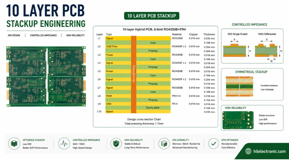
10 Layer PCB Stackup Design for Impedance and Planes
Figure 1. 10 layer PCB stackup for impedance and plane...
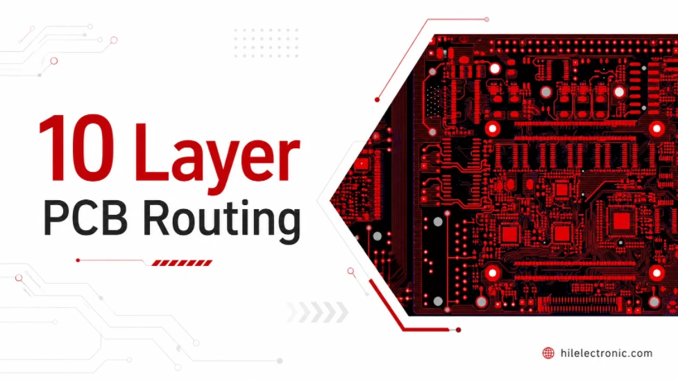
10 Layer PCB Routing Rules for DDR5, PCIe and Crosstalk
Figure 1. 10 layer PCB routing rules for DDR5 PCIe and...
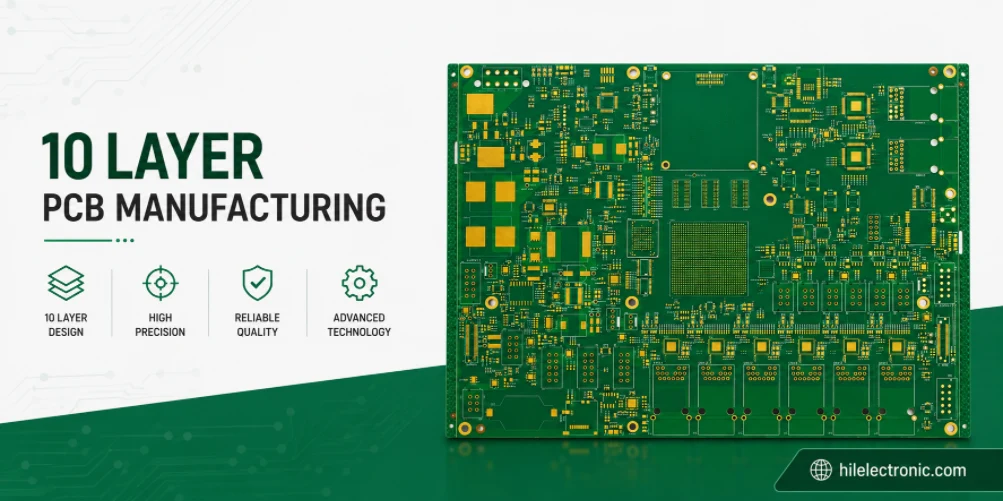
10 Layer PCB Manufacturer for Rigid, Flex and Rigid-Flex
Figure 1. 10 layer PCB manufacturer production capability....
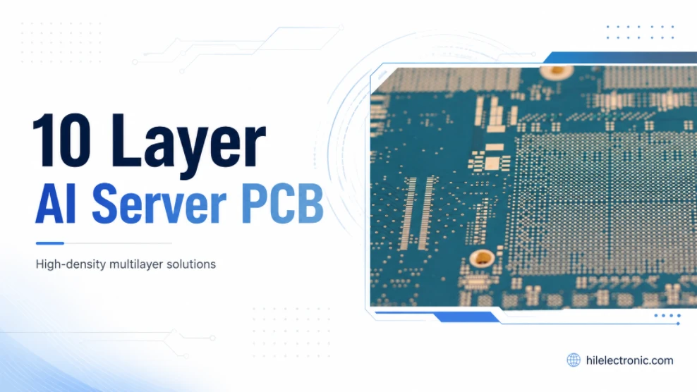
10 Layer AI Server PCB Engineering for Accelerator Hardware
Figure 1. 10 layer AI server PCB for accelerator hardware....
How to get a quote for PCBs
Let‘s run DFM/DFA analysis for you and get back to you with a report. You can upload your files securely through our website. We require the following information in order to give you a quote:
-
- Gerber, ODB++, or .pcb, spec.
- BOM list if you require assembly
- Quantity
- Turn time
In addition to PCB manufacturing, we offer a comprehensive range of electronic services, including PCB design, PCBA, and turnkey solutions. Whether you need help with prototyping, design verification, component sourcing, or mass production, we provide end-to-end support to ensure your project’s success.
For PCBA services, please provide your BOM (Bill of Materials) and any specific assembly instructions. We also offer DFM/DFA analysis to optimize your designs for manufacturability and assembly, ensuring a smooth production process.