
Heavy Copper PCB Thermal Management: Design Strategies for High-Power Applications

Introduction
Heavy copper PCBs have become indispensable in high-power electronics, where current densities exceed what standard circuit boards can safely handle. These specialized boards utilize copper layers ranging from 3oz to 20oz per square foot, enabling superior current-carrying capacity for applications like industrial motor drives, renewable energy converters, and automotive power systems.
However, concentrated power dissipation creates significant thermal challenges that directly impact reliability, operational lifespan, and performance stability. This article examines the critical heavy copper PCB thermal management strategies that enable designs to maintain efficiency and durability under demanding conditions.
The Role of Thermal Management in Heavy Copper PCBs
Thermal Challenges in High-Power Designs
Heat dissipation in heavy copper PCBs presents unique challenges compared to conventional boards. High current densities generate substantial I²R losses, while power semiconductors concentrate heat in localized areas, often exceeding 100W/cm². Without adequate thermal pathways, junction temperatures rise rapidly, accelerating electromigration and material degradation.
Thermal Performance Advantages
The fundamental difference between standard and heavy copper boards lies in thermal mass and spreading capability. Thicker copper planes conduct heat more effectively in lateral directions, creating wider distribution zones that reduce hotspot formation. This enhanced thermal conductivity becomes critical when multiple power devices operate simultaneously.
Heat Flow Path Design
Understanding the thermal path defines successful power electronics PCB design:
- Component level – Heat transfers from semiconductor junctions through die attach materials into copper planes
- Board level – Thermal energy spreads laterally through heavy copper layers and vertically through thermal vias
- System level – Heat moves through the substrate to external cooling mechanisms or heatsinks
- Interface optimization – Each resistance point in this chain must be minimized to prevent thermal bottlenecks
Understanding Copper Thickness and Heat Conduction
Copper Thickness vs. Thermal Conductivity
Copper thickness directly influences both current capacity and thermal performance. Standard 1oz copper (35μm) offers baseline conductivity of 400 W/m·K, while 4oz copper (140μm) provides four times the cross-sectional area for heat spreading. Comparative analysis shows 2oz copper handles approximately 3A per mm width at 10°C temperature rise, while 6oz copper extends this to 6-7A under identical conditions.
Thermal and Mechanical Considerations
The increased vertical copper mass enhances z-axis thermal conduction, particularly important for transferring heat from surface-mounted power devices to internal planes. Beyond 10oz thickness, diminishing returns appear as substrate thermal resistance becomes dominant. Additionally, mechanical stress from thermal expansion mismatch increases with copper weight, requiring careful material selection to prevent delamination or barrel cracking in thermal vias.
Heat Path Design and Via Optimization for Heavy Copper PCB Thermal Management
Thermal Via Array Configuration
Thermal via arrays beneath power components create critical z-axis conduction paths. Optimal configurations place 0.3-0.5mm diameter vias on 0.8-1.2mm pitch directly under heat-generating devices. Via density must balance thermal performance against manufacturing constraints and signal integrity requirements.
Heat Spreading Path Engineering
Multiple copper layers interconnected through staggered via fields create three-dimensional thermal networks. This approach distributes localized heat into broader board areas, effectively lowering peak temperatures. Power plane segmentation must consider both current return paths and thermal spreading requirements to avoid creating thermal islands.
Copper Inlay and Embedded Structures
Copper coin technology embeds thick copper slugs (typically 1-3mm thick) into routed PCB cavities, creating direct thermal highways from component mounting surfaces to heatsinks or metal cores. These structures reduce thermal resistance by 40-60% compared to standard via arrays, particularly effective for high-density power modules where surface area limitations restrict conventional spreading.
Via Filling for Enhanced Conductivity
Thermal via filling with conductive epoxy or copper plating eliminates air gaps that impede heat transfer. Filled vias also improve reliability by preventing solder wicking during assembly and reducing coefficient of thermal expansion mismatches between board layers.

Heavy Copper PCBs
Thermal Interface Materials and Conductive Substrates
High-Performance Base Materials
Material selection fundamentally determines heavy copper PCB thermal management effectiveness. Thermally enhanced FR-4 variants incorporate ceramic fillers achieving 1-3 W/m·K, doubling standard FR-4 performance (0.3-0.4 W/m·K) while maintaining cost advantages and processability for multilayer constructions.
Metal Core PCB Integration
Metal core PCBs utilize aluminum or copper bases with dielectric isolation layers, achieving thermal conductivities of 1.5-8 W/m·K depending on dielectric thickness. These structures excel in applications requiring direct thermal paths to chassis or forced-air cooling systems, though electrical isolation requirements limit layer count and routing density.
Ceramic Substrates for Extreme Conditions
Aluminum nitride substrates provide thermal conductivity exceeding 170 W/m·K, while alumina offers approximately 25 W/m·K. These materials enable heavy copper designs operating at extreme temperatures or requiring minimal thermal expansion (CTE matching to semiconductors), though cost considerations limit applications to mission-critical systems.
Structural and Layout Considerations
Thermal Design Layout Principles
Component placement strategy directly impacts thermal balance across heavy copper PCBs. Distributing power devices according to thermal load analysis prevents localized overheating. Maintaining minimum 5-8mm spacing between high-dissipation components allows adequate copper spreading zones to function effectively.
Heat Spreading Zone Implementation
Dedicated copper pour areas without routing restrictions maximize lateral heat conduction:
- Inner layer zones – Solid copper planes sized according to power dissipation maps
- Via connectivity – Dense via arrays ensure efficient heat collection from surface layers
- Thermal symmetry – Balanced copper distribution prevents board warping during operation
- Area calculation – Spreading zones typically sized at 3-5× the component footprint area
Multilayer Architecture for Heavy Copper PCB Thermal Management
Symmetrical copper distribution across layer stacks creates parallel thermal paths while maintaining mechanical stability. Alternating signal and power plane configurations in 6-10 layer heavy copper boards optimize thermal networks without compromising signal integrity. Each additional copper layer contributes incremental thermal capacity, with optimal returns typically achieved in 6-8 layer designs.
Manufacturing Techniques for Enhanced Thermal Performance
Heavy Copper Plating Processes
Precision electroplating builds uniform copper thickness across panel surfaces and through-hole barrels. Current density control during plating determines copper grain structure and resulting thermal conductivity. Multi-step plating sequences achieve heavy copper PCB manufacturing tolerances within ±10% thickness variation across panels.
Advanced Fabrication Methods
Step plating techniques create varying copper weights on different board areas, optimizing thermal performance where needed while reducing material costs elsewhere. Differential etching compensates for increased copper thickness during pattern formation, maintaining trace geometry accuracy within ±0.05mm for critical thermal paths.
Embedded Copper Integration
Copper coin installation demands precise cavity milling (typically ±0.1mm tolerance) and pressure bonding to eliminate air gaps at thermal interfaces. Subsequent plating fills gaps between embedded structures and surrounding copper layers, creating continuous thermal paths. Manufacturing quality directly determines interface resistance and long-term thermal cycling reliability.
Application Insights
Power Module PCB Applications
Industrial motor controllers and renewable energy inverters leverage heavy copper thermal management to sustain continuous operation at 150-200A load currents. Multi-kilowatt designs integrate copper inlays with forced convection cooling, achieving junction temperatures below 125°C under full load conditions across ambient temperatures up to 85°C.
Automotive Power Electronics
Electric vehicle inverters require heavy copper PCBs managing 400-800V bus voltages and 300-600A phase currents. Thermal designs combine 8-12oz copper layers with direct liquid cooling interfaces, supporting power densities exceeding 50kW per board while meeting automotive reliability standards over 15-year operational lifespans and temperature cycling from -40°C to +125°C.
Communication Infrastructure
Telecom base station power amplifiers utilize heavy copper boards dissipating 200-500W across compact form factors. Metal core substrates with embedded thermal vias transfer heat to chassis-mounted cooling plates, maintaining RF performance stability and efficiency across -40°C to +85°C operating ranges.
Conclusion
Effective heavy copper PCB thermal management requires integrated approaches addressing material selection, copper weight distribution, via architecture, and heat spreading path optimization. Designs that systematically minimize thermal resistance from junction to ambient enable reliable operation of increasingly powerful electronic systems. As power densities continue rising across industrial, automotive, and infrastructure applications, thermal engineering becomes inseparable from electrical design in achieving both performance targets and reliability requirements.
Highleap Electronics Thermal Management Capabilities
Highleap Electronics specializes in precision heavy copper PCB manufacturing with comprehensive thermal optimization support:
- Heavy copper fabrication – Production capability from 3oz to 20oz copper weight with ±10% thickness control
- Advanced thermal structures – Thermal via arrays, embedded copper coins, and hybrid metal core constructions
- Material expertise – Thermally enhanced FR-4, aluminum/copper core substrates, and ceramic base options
- Engineering support – Thermal simulation assistance and design optimization recommendations for power electronics
- Quality assurance – Thermal cycling testing and thermal resistance verification for critical applications
Contact our engineering team to discuss how our heavy copper PCB thermal management capabilities can enhance reliability and performance in your next high-power project.

Recommended Posts
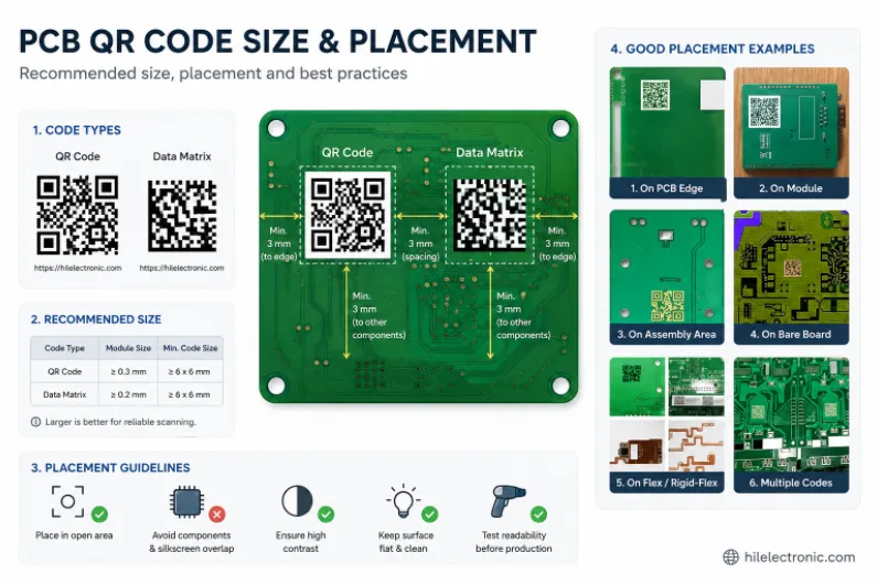
PCB QR Code Size and Placement: Design Rules for Reliable Scanning
Figure 1. PCB QR code size and placement image for PCB...
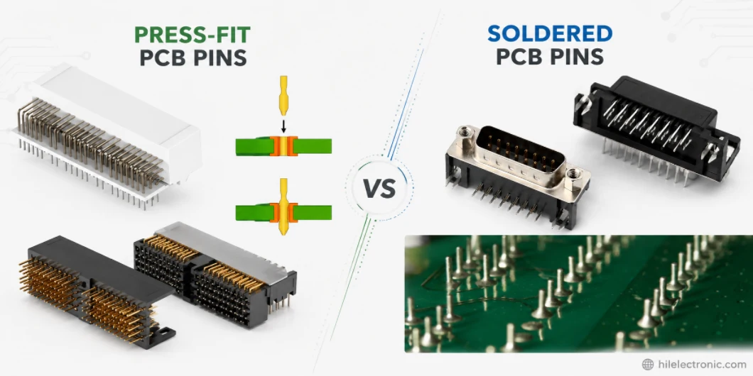
Press-Fit vs Soldered PCB Pins: Header, Connector, and Through-Hole Choices
Figure 1. press-fit vs soldered PCB pins image for PCB...
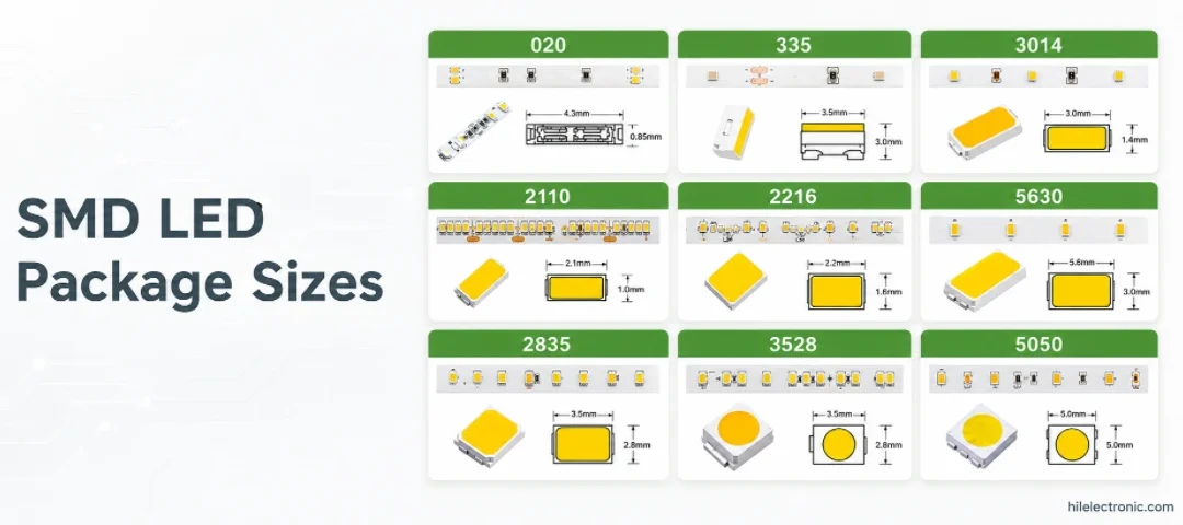
SMD LED Package Sizes: 2835 vs 5050 vs 3528 and PCB Selection
Figure 1. SMD LED package sizes image for PCB...
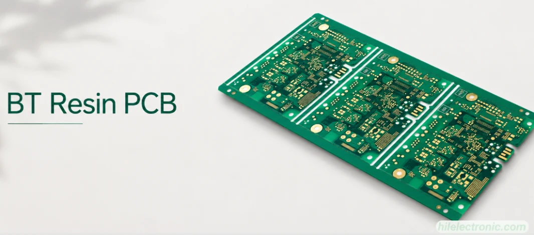
BT Resin PCB: Properties, Uses, and Fabrication Controls
Figure 1. BT resin PCB image for PCB manufacturing...
How to get a quote for PCBs
Let‘s run DFM/DFA analysis for you and get back to you with a report. You can upload your files securely through our website. We require the following information in order to give you a quote:
-
- Gerber, ODB++, or .pcb, spec.
- BOM list if you require assembly
- Quantity
- Turn time
In addition to PCB manufacturing, we offer a comprehensive range of electronic services, including PCB design, PCBA, and turnkey solutions. Whether you need help with prototyping, design verification, component sourcing, or mass production, we provide end-to-end support to ensure your project’s success.
For PCBA services, please provide your BOM (Bill of Materials) and any specific assembly instructions. We also offer DFM/DFA analysis to optimize your designs for manufacturability and assembly, ensuring a smooth production process.