
Reflow Soldering: Principles, Process, and Key Considerations for SMT Assembly

Introduction
Reflow soldering is the dominant soldering method in surface mount technology (SMT), enabling precise and reliable attachment of components to printed circuit boards. By applying controlled heat to melt solder paste deposited on PCB pads, this process creates permanent metallurgical bonds between component terminals and board surfaces.
This article provides a comprehensive examination of reflow soldering fundamentals, thermal zone design, equipment options, process parameters, and defect mitigation strategies essential for high-quality electronics manufacturing.
Reflow Soldering Definition and Background
Reflow soldering is a thermal process that melts pre-applied solder paste under a controlled temperature profile, forming permanent solder joints between SMT components and PCB pads upon cooling.
Unlike wave soldering, which passes boards through a molten solder wave primarily for through-hole components, reflow soldering applies localized heat uniformly across the entire assembly. This makes it ideally suited for fine-pitch surface mount devices, BGAs, and high-density interconnect boards where precision and thermal control are critical.
Reflow Soldering Process Principles
Thermal Cycle and Solder Paste Reaction Mechanism
Solder paste consists of metal alloy powder suspended in flux and a carrier medium. During reflow, controlled heating activates the flux to remove surface oxides from both pads and component leads while reducing surface tension. This enables molten solder to wet metallized surfaces and form intermetallic compounds at the interface. The quality of these reactions depends critically on achieving proper time-above-liquidus (TAL) within a precisely controlled thermal profile.
Staged Thermal Zone Design
The reflow soldering process is fundamentally a controlled thermal treatment divided into distinct heating and cooling phases. Each zone serves a specific metallurgical purpose, and the transition between zones must be carefully managed to ensure uniform temperature distribution across components of varying thermal masses.
| Zone | Purpose | Characteristics |
|---|---|---|
| Preheat | Gradual temperature rise; minimizes thermal shock; volatilizes solvents | Linear temperature ramp |
| Thermal Soak | Equalizes PCB and component temperatures; activates flux; expels volatiles | Temperature plateau |
| Reflow (Peak) | Melts solder alloy above liquidus; enables wetting of joint surfaces | Peak temperature |
| Cooling | Solidifies molten solder; forms stable metallurgical bond | Controlled descent |
The critical factors in thermal profile design are not peak temperature alone, but rather the ramp rates, time above liquidus (TAL), cooling rate, and overall thermal uniformity across the assembly.
Reflow Soldering Equipment and Technical Variants
Reflow Oven Types
Convection Reflow Ovens
Forced convection ovens use heated air circulation to transfer thermal energy uniformly to PCB assemblies. This technology dominates modern SMT production due to its excellent temperature distribution and compatibility with diverse board configurations.
Infrared (IR) Reflow Ovens
IR ovens heat assemblies through radiant energy transfer. While capable of rapid heating, they can produce uneven temperature distribution based on component color and mass variations, limiting their application to less demanding assemblies.
Vapor Phase Reflow Systems
These systems transfer heat through condensation of an inert, high-boiling-point fluid. The phase-change mechanism provides inherently uniform heating regardless of component geometry, making it valuable for thermally challenging assemblies with significant mass variation.
Nitrogen-Assisted Reflow Soldering
Introducing nitrogen atmosphere reduces oxygen concentration in the reflow chamber, minimizing oxidation of solder and pad surfaces during the heating cycle. This improves wetting behavior and joint reliability, making nitrogen assist particularly valuable for automotive, aerospace, and other high-reliability applications.

SMT Reflow Ovens
Reflow Soldering Process Workflow
Preparation and Pre-Processing
Prior to reflow, PCBs undergo cleaning to remove contaminants that could interfere with solder wetting. Solder paste is then deposited through stencil printing onto designated pads with controlled volume and alignment. SMT components are subsequently placed onto the paste deposits using high-precision pick-and-place equipment.
Reflow Thermal Cycle
The loaded assembly passes through the reflow oven’s sequential thermal zones. Precise control of conveyor speed and zone temperatures ensures adherence to the developed thermal profile. Temperature monitoring via thermocouples attached to test boards validates that all areas of the assembly experience the intended thermal exposure.
Post-Processing and Inspection
Following cooling, assemblies undergo quality verification through visual inspection, automated optical inspection (AOI), and X-ray examination for hidden joints such as BGAs. These inspection methods detect solder defects before boards proceed to subsequent assembly or functional testing stages.
Critical Reflow Soldering Parameters and Control
Optimal reflow soldering results require careful management of several interdependent parameters. These values must be tailored to specific board designs, paste formulations, and component thermal characteristics rather than applied as universal constants.
| Parameter | Impact on Solder Joint Quality |
|---|---|
| Ramp Rate | Affects thermal shock risk and paste volatile release behavior |
| Peak Temperature | Determines complete solder melting and intermetallic formation |
| Time Above Liquidus (TAL) | Influences wetting completeness and joint metallurgical integrity |
| Cooling Rate | Controls intermetallic compound growth and mechanical strength |
Common Reflow Soldering Defects and Root Cause Analysis
Understanding the relationship between process conditions and defect formation enables targeted corrective action. The following defects represent common failure modes in reflow soldering operations.
| Defect | Potential Root Causes |
|---|---|
| Tombstoning | Uneven thermal distribution; asymmetric paste deposition; pad design imbalance |
| Solder Bridging | Excessive paste volume; stencil aperture design errors; component misalignment |
| Voiding | Trapped outgassing; inadequate soak time; paste formulation issues |
| Cold Joints | Insufficient peak temperature; inadequate time above liquidus |
Effective defect resolution requires analysis of multiple factors including thermal profile data, paste characteristics, stencil design, and flux activity levels.
Advanced Reflow Soldering Techniques and Trends
Automated Thermal Profiling
Modern reflow systems incorporate real-time monitoring and automated profile optimization capabilities. These systems continuously adjust zone temperatures and conveyor speeds to maintain target thermal exposure despite variations in incoming board thermal mass.
Lead-Free Solder Considerations
Lead-free alloys such as SAC (tin-silver-copper) require higher peak temperatures and narrower process windows compared to traditional tin-lead formulations. These materials demand more precise thermal control and often benefit from nitrogen atmosphere processing.
High-Density and BGA Assembly Challenges
Increasing component density and hidden-joint packages like BGAs intensify requirements for thermal uniformity and inspection capability. Advanced reflow strategies address these challenges through optimized zone design, extended soak profiles, and comprehensive X-ray verification protocols.
Conclusion
Reflow soldering represents an integration of thermal engineering and materials science essential to modern electronics assembly. Achieving reliable solder joints requires systematic attention to thermal profile development, paste printing accuracy, component placement precision, and rigorous process control.
A thorough understanding of reflow soldering principles enables engineers to optimize PCB assembly operations and deliver products meeting the highest reliability standards.

Recommended Posts
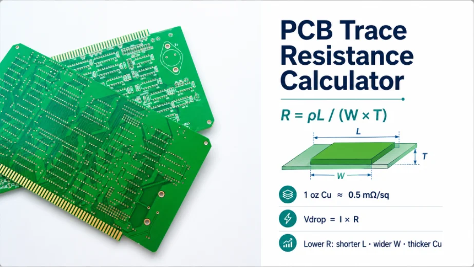
PCB Trace Resistance Calculator: How to Calculate Trace Resistance and Voltage Drop
Figure 1. PCB trace resistance affects voltage drop, heat...
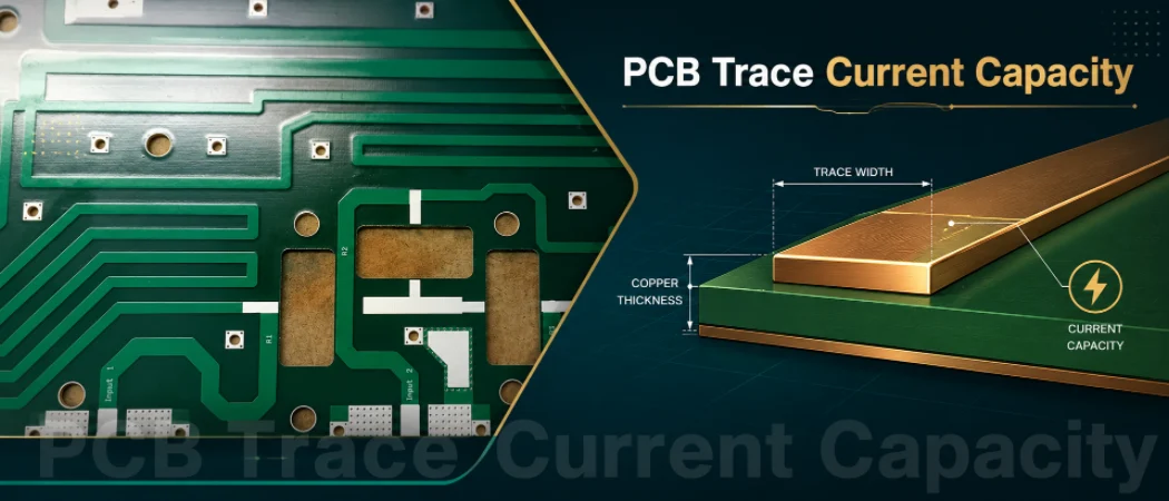
PCB Trace Current Capacity: Width, Copper Weight, and IPC-2221
Figure 1. PCB trace current capacity depends on copper...

EAGLE PCB Software: Is It Free, EAGLE vs KiCad, and How to Export Gerber Files
Figure 1. EAGLE PCB software projects should be exported...

Microcontroller Board Soldering and Programming: QFN Pads, SWD, and FTDI Drivers
Figure 1. Microcontroller board soldering and programming...
How to get a quote for PCBs
Let‘s run DFM/DFA analysis for you and get back to you with a report. You can upload your files securely through our website. We require the following information in order to give you a quote:
-
- Gerber, ODB++, or .pcb, spec.
- BOM list if you require assembly
- Quantity
- Turn time
In addition to PCB manufacturing, we offer a comprehensive range of electronic services, including PCB design, PCBA, and turnkey solutions. Whether you need help with prototyping, design verification, component sourcing, or mass production, we provide end-to-end support to ensure your project’s success.
For PCBA services, please provide your BOM (Bill of Materials) and any specific assembly instructions. We also offer DFM/DFA analysis to optimize your designs for manufacturability and assembly, ensuring a smooth production process.