
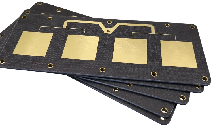
China Taconic TLX-8 PCB Manufacturer | Custom PTFE Fabrication

When routing layouts for phased array antennas, aerospace telemetry, and microwave radar systems, engineers specify woven-glass reinforced PTFE laminates to minimize dielectric loss. Taconic TLX-8 is a premier substrate for these applications, offering mechanical stability combined with the extreme low-loss characteristics of Teflon.
However, transitioning a Dk 2.55 microwave design from software simulation into a physical board requires navigating severe chemical and mechanical bottlenecks. Because PTFE substrates are notoriously hostile to standard factory chemical lines, sending Gerber files without strict Design for Manufacturability (DFM) considerations will lead to trace undercutting and plating voids. As an experienced China Taconic TLX-8 PCB manufacturer, Highleap Electronics has compiled this technical workflow. Review these 8 critical fabrication realities before submitting your project to ensure first-pass success.
Request a Taconic TLX-8 PCB Fabrication Quote
DFM Table of Contents
- Specs for a TLX-8 Microwave Printed Circuit Board
- Trace Etching in TLX-8 Low Loss Board Fabrication
- Custom Taconic TLX-8 PTFE PCB Manufacturing Challenges (Deep Dive)
- Dimensional Scaling for Taconic TLX-8 Circuit Board Makers
- Hybrid Stackups: Lowering Your Taconic TLX-8 PCB Fabrication Quote
- Surface Finishes from a Taconic TLX-8 Antenna PCB Supplier
- Lead Times for a Taconic TLX-8 Microwave PCB Prototype
- Turnkey PCBA from a Taconic TLX-8 RF PCB Factory
Specs for a TLX-8 Microwave Printed Circuit Board
Before calculating trace widths, hardware teams must baseline the physical limits of the material. When engineering a TLX-8 microwave printed circuit board, the mechanical properties dictate long-term reliability just as much as the electrical specs. By exploring our PCB laminate material selection, engineers prioritize TLX-8 for three critical baseline metrics:
- Stable Dk & Df: The dielectric constant is tightly controlled at 2.55 ± 0.04, and the dissipation factor is 0.0019 (at 10 GHz). This guarantees consistent 50-ohm matching across different manufacturing lots.
- Moisture Resistance: An extremely low moisture absorption rate of 0.02% eliminates the risk of impedance shifts in high-humidity outdoor antenna enclosures.
- Z-Axis CTE: The woven fiberglass stabilizes the PTFE, keeping the Z-axis thermal expansion close to copper (24 ppm/°C). This prevents plated through-holes (PTH) from fracturing during thermal shock.
Trace Etching in TLX-8 Low Loss Board Fabrication
In TLX-8 low loss board fabrication, the low dielectric constant means your RF traces will naturally be wider than those on standard FR-4 to hit the same impedance targets. However, the etching process on soft PTFE requires extreme precision.
We strongly advise using 0.5 oz or 1 oz copper for your RF layers. Do not specify 2 oz copper. Etching heavy copper requires extended chemical exposure, which undercuts the trace sidewalls, creates a trapezoidal profile, and destroys your millimeter-wave impedance targets. Highleap utilizes Laser Direct Imaging (LDI) to hold trace width tolerances tightly, ensuring exact correlation with your HFSS simulation software.
Custom Taconic TLX-8 PTFE PCB Manufacturing Challenges (Deep Dive)
This is the absolute bottleneck of microwave board manufacturing and the primary reason standard board houses fail at fabricating Teflon-based laminates. The exact chemical properties that give Taconic TLX-8 its incredible low-loss electrical performance also make it highly chemically inert and natively hydrophobic.
The Fluoropolymer Plating Problem
In standard fabrication, after a via is drilled, it is placed in an alkaline permanganate bath to clean out resin smear before liquid copper is deposited. If a factory attempts this on a custom Taconic TLX-8 PTFE PCB, the liquid copper plating solution will bead up and roll completely off the Teflon hole wall. The carbon-fluorine bonds in the PTFE matrix repel liquids entirely. Without intervention, this leads to massive plating voids. When the board later passes through an SMT reflow oven, trapped moisture in these voids will rapidly outgas, blowing any weak copper plating right off the via wall.
Wet Process: Sodium Naphthalene Etching
To successfully metallize these vias, we must execute a complex fluoropolymer activation process. The most reliable wet-process method is sodium naphthalene etching. The drilled PCB panel is submerged in a highly reactive sodium complex. The sodium acts as a violent reducing agent, physically tearing the fluorine atoms away from the carbon backbone. This leaves behind a microscopic, carbon-rich sponge texture that is highly hydrophilic. When the board enters the electroless copper line, the palladium catalyst anchors securely into this modified layer.
Dry Process: Vacuum Plasma Desmear
For high-density interconnect designs or microvias where viscous sodium liquids cannot penetrate, we utilize vacuum plasma chambers. By ionizing a mixture of Helium, Oxygen, and CF4 gases with RF energy, the resulting plasma physically bombards and micro-roughens the inert PTFE surface, ensuring IPC Class 3 via reliability.
Dimensional Scaling for Taconic TLX-8 Circuit Board Makers
Despite the fiberglass reinforcement, PTFE is a soft polymer that stores internal mechanical stress from the raw lamination process. During multilayer bare board fabrication, when we etch away the copper planes, these stresses are released, causing the material to microscopically stretch or shrink.
If uncompensated, internal layer pads will misalign with the CNC drill hits. Any reliable Taconic TLX-8 circuit board maker must resolve this by running “first article” scaling test panels. Our CAM engineers calculate precise X/Y dimensional scaling compensation factors and apply them to your Gerber data before imaging, guaranteeing perfect layer-to-layer registration.
Hybrid Stackups: Lowering Your Taconic TLX-8 PCB Fabrication Quote
Using TLX-8 for an entire 8-layer board is often an unnecessary drain on your procurement budget. Most modern RF modules require microwave routing on the outer layers, with digital logic and power on the inside.
To optimize your Taconic TLX-8 PCB fabrication quote, we highly recommend asymmetric hybrid stackups. We utilize TLX-8 for the outer layers and press it together with cost-effective, high-Tg FR-4 (like Isola 370HR) for the internal digital layers. By applying highly customized thermal press recipes, we successfully co-cure these dissimilar materials without inducing asymmetric warpage (the potato-chip effect).
DFM Guideline: Prepreg Selection for Hybrid Builds
When designing a hybrid stackup, do not use PTFE bonding films to bond FR-4 to TLX-8, as the lamination temperatures are fundamentally incompatible. Instead, use high-Tg epoxy prepregs or specialized low-loss thermoset prepregs to ensure a reliable, flat lamination cycle.
Surface Finishes from a Taconic TLX-8 Antenna PCB Supplier
The surface finish you specify directly impacts insertion loss due to the skin effect at microwave frequencies. As a leading Taconic TLX-8 antenna PCB supplier, we strongly recommend Immersion Silver or ENEPIG (Electroless Nickel Electroless Palladium Immersion Gold).
Immersion Silver provides the absolute lowest insertion loss for high-frequency RF paths, while ENEPIG offers perfectly flat pads for bare-die wire bonding. Avoid HASL entirely, as the uneven solder topography will severely disrupt your high-frequency signals.
Lead Times for a Taconic TLX-8 Microwave PCB Prototype
Because PTFE requires specialized plasma desmear and precise dimensional scaling, lead times are naturally longer than standard FR-4. When you submit your Gerber files for a Taconic TLX-8 microwave PCB prototype, our CAM department performs a rigorous DFM check.
We cross-reference your trace widths against our advanced high-frequency PCB etching tolerances. By utilizing Polar Instruments, we verify your 50-ohm single-ended and 100-ohm differential impedance calculations, ensuring the physical board will perform exactly as simulated before a single panel is cut.
Turnkey PCBA from a Taconic TLX-8 RF PCB Factory
Teflon laminates are incredibly susceptible to surface scratches and handling damage. Moving a bare RF board from a fabricator to a separate third-party assembly house introduces severe logistical risks. A single scratch across a critical RF trace alters the impedance, ruining the board.
To eliminate supplier finger-pointing, Highleap Electronics operates as a comprehensive Taconic TLX-8 RF PCB factory. We seamlessly transition your project from our wet processing lines directly into our aerospace-grade PCBA manufacturing facility. By keeping your project under one roof, we maintain strict environmental controls and utilize 3D X-Ray (AXI) to guarantee void-free thermal grounding beneath high-power RF transceivers. Contact our engineers today to launch your next microwave project.

Recommended Posts

PCB Laminate Lead Time and Production Scheduling
On this page Why Laminate Lead Times Vary Standard vs...
Low Dk Low Df PCB Material for High Speed Signals
Figure 1. Low loss PCB material selection for high speed...

PCB Price Increase in 2026: Key Reasons and Industry Trends
Figure 1. PCB Price Increase Table of Contents Why Are PCB...
10 Layer PCB Materials for FR-4, Low-Loss and RF Boards
Figure 1. 10 layer PCB materials for FR-4 low-loss and RF...
How to get a quote for PCBs
Let us run DFM/DFA analysis for you and get back to you with a report.
You can upload your files securely through our website.
We require the following information in order to give you a quote:
-
- Gerber, ODB++, or .pcb, spec.
- BOM list if you require assembly
- Quantity
- Turn time