
Automotive HDI PCB for ADAS, Radar & Power Control Systems

Introduction
The automotive electronics landscape has transformed dramatically with the rapid advancement of Advanced Driver Assistance Systems (ADAS), autonomous driving technologies, vehicle radar systems, and electric powertrain control modules. These sophisticated systems demand exceptional signal density, uncompromising reliability, efficient thermal management, and optimal space utilization within increasingly compact vehicle architectures.
Automotive HDI PCB provides high-density interconnection solutions for next-generation ADAS and radar systems, addressing these critical design challenges. The transition from conventional printed circuit boards to high-density interconnect technology represents a fundamental shift in how automotive electronics achieve the performance and reliability standards required for modern vehicle safety and functionality.
Why Automotive HDI PCB Technology is Essential
High-Speed Data Transmission Requirements
Millimeter-wave radar systems operating at 77 GHz and 79 GHz, multi-camera arrays, and LiDAR sensors generate massive data streams that require precise signal routing with minimal loss. Automotive HDI PCB technology enables these transmissions through laser-drilled microvias that create shorter signal paths, reducing impedance discontinuities and maintaining signal integrity. The stacked microvia architecture minimizes stub lengths and provides controlled impedance paths essential for radar and high-resolution camera processing units.
Space Optimization in Vehicle Modules
Modern vehicle electronic control units (ECUs) and sensor modules must deliver expanding functionality within shrinking physical footprints. HDI PCB technology achieves component density increases through sequential lamination, blind and buried via structures, and fine-line routing capabilities down to 75 micrometers. This miniaturization allows automotive designers to integrate more processing power, memory, and sensor interfaces within mirror housings, pillar modules, and dashboard assemblies.
Reliability in Harsh Automotive Environments
Automotive electronics endure temperature cycling from -40°C to +125°C, continuous mechanical vibration, humidity exposure, and electromagnetic interference far exceeding consumer electronics standards. Automotive HDI PCB designs incorporate advanced dielectric materials with superior thermal stability, matched coefficient of thermal expansion properties, and laser-drilled microvias with enhanced copper plating that withstands thousands of thermal cycles.
Automotive HDI PCB Design Considerations
Material Selection for Extreme Conditions
The substrate materials used in automotive HDI PCB fabrication must meet stringent automotive qualification standards while maintaining electrical performance across extreme operating conditions. Material requirements include:
- High glass transition temperature – Tg values above 170°C ensure dimensional stability during assembly and operation.
- Low moisture absorption – Minimizes dielectric constant shifts and delamination risks in humid environments.
- Thermal stability – Materials such as high-performance FR-4, Rogers laminates, and MEGTRON series maintain properties across automotive temperature ranges.
These materials support compliance with AEC-Q200 reliability standards and IATF16949 quality requirements essential for automotive supply chain integration.
Microvia Architecture and Reliability
The microvia structure defines the reliability ceiling for automotive HDI PCB assemblies. Structure selection between 1+n+1 and 2+n+2 configurations depends on routing density and reliability requirements. Copper-filled microvias with electroplated sidewalls provide superior mechanical strength compared to resin-filled alternatives, particularly for power distribution networks in electric vehicle controllers.
Achieving uniform copper plating thickness and matched coefficient of thermal expansion between layers requires precise process control during sequential lamination cycles. Drilling parameters and desmear chemistry directly influence long-term via reliability under thermal cycling conditions.
Thermal Management Strategies
Electric motor controllers and battery management systems must dissipate significant heat while maintaining stable power delivery. Strategic copper weight distribution across power and ground layers, combined with thermal via arrays beneath high-power semiconductors, creates efficient heat transfer paths. Metal-core HDI PCB variants integrate aluminum substrates with HDI buildup layers for applications requiring direct thermal interface with cooling systems.
Signal Integrity and EMI Control
High-speed differential pairs carrying SerDes data, automotive Ethernet, or radar signals require meticulous attention to trace geometry and reference plane continuity. Ground plane layers positioned adjacent to signal layers provide electromagnetic shielding that reduces crosstalk between sensitive analog sensor inputs and noisy digital processing circuits. Low dielectric constant materials minimize signal propagation delays and maintain tight impedance tolerances essential for multi-gigabit data transmission.

Automotive HDI PCB Applications
ADAS and Autonomous Driving Systems
Front-facing camera control boards and radar signal processing units represent the most demanding automotive HDI PCB applications. These modules integrate image sensors, FPGA or ASIC processors, power management, and multiple communication interfaces on compact HDI substrates. Blind via technology enables component placement on both sides while maintaining signal integrity, supporting the miniaturization required for integration into mirror housings, grille assemblies, and roof-mounted sensor pods.
Electric Powertrain and Battery Management
Electric vehicle inverters, motor controllers, and battery management systems utilize automotive HDI PCB designs to handle high current power distribution alongside sensitive voltage and temperature monitoring circuits. The multilayer HDI construction allows segregation of high-power switching circuits from low-noise analog measurement channels through strategic layer assignment. Battery management controllers particularly benefit from HDI routing density, enabling direct connections to hundreds of cell monitoring points while maintaining required isolation.
Connectivity and Infotainment Modules
Central display controllers, telematics modules, and wireless connectivity hubs require automotive HDI PCB technology to support high-resolution video interfaces and multiple radio frequency bands within dashboard-mounted enclosures. These applications leverage fine-pitch component mounting capabilities enabled by microvias, allowing direct connections to advanced application processors with ball-grid-array packages at 0.4mm pitch or finer.

Manufacturing and Quality Standards for Automotive HDI PCB
Production Challenges
The production of automotive HDI PCB assemblies requires specialized capabilities beyond standard multilayer fabrication. Multiple press cycles with aligned registration, controlled depth laser via formation, and uniform copper deposition across varied via densities challenge manufacturing consistency. Critical manufacturing requirements include:
- Sequential lamination precision – Multiple lamination cycles with registration tolerance below 75 micrometers maintain via alignment.
- Laser drilling control – Depth control within ±10 micrometers ensures consistent microvia formation without substrate damage.
- Copper plating uniformity – Achieving consistent thickness across high-density via fields prevents reliability failures.
Quality Assurance and Testing
Automotive specifications demand comprehensive inspection protocols to verify manufacturing quality and predict long-term reliability. Automated optical inspection (AOI) validates microvia formation quality and captures dimensional data for process control. Flying probe testing verifies electrical continuity across complex routing without dedicated test fixtures. X-ray inspection analyzes internal via structure and copper fill quality not visible through surface inspection.
Accelerated thermal cycling validation subjects automotive HDI PCB assemblies to temperature extremes exceeding operational requirements, typically 1000 cycles from -40°C to +125°C, to predict long-term reliability. Quality management systems certified to IATF16949 provide the framework for manufacturing traceability and process control required by automotive OEMs and tier-one suppliers.
Conclusion
Automotive HDI PCB technology has become indispensable for meeting the density, reliability, and performance requirements of modern vehicle electronics. The combination of fine-line routing, stacked microvia structures, and advanced substrate materials enables automotive designers to achieve functionality levels impossible with conventional PCB technology while maintaining the robustness required for decades of operation under harsh environmental conditions.
Highleap Electronics delivers comprehensive automotive HDI PCB solutions with proven capabilities:
- IATF16949-certified manufacturing – Full compliance with automotive quality management systems and traceability requirements.
- Advanced HDI technology – Sequential lamination capabilities supporting 1+n+1 and 2+n+2 microvia structures with laser drilling precision.
- Reliability verification – Thermal cycling testing, microsection analysis, and accelerated life testing to automotive standards.
- Design support – Engineering collaboration to optimize HDI stack-ups for manufacturability while meeting stringent automotive performance requirements.
Partner with Highleap Electronics for your automotive HDI PCB projects and benefit from our expertise in ADAS, radar systems, power control modules, and battery management applications. Contact our engineering team to discuss your automotive PCB requirements and ensure first-pass success in this demanding market segment.

Recommended Posts
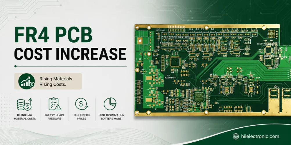
FR4 PCB Cost Increase for Electronics Manufacturers
Table of contents Why FR4 Prices Continue to Rise Raw...
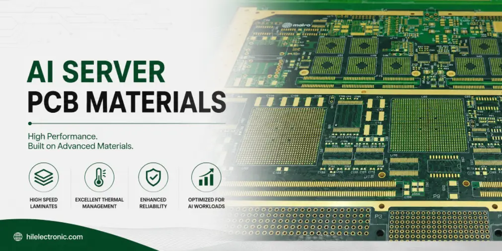
AI Server PCB Materials: Low-Loss Laminates, Stack-Up, Thermal and PCBA Guide
On this page What AI Server PCB Materials Need to Solve...
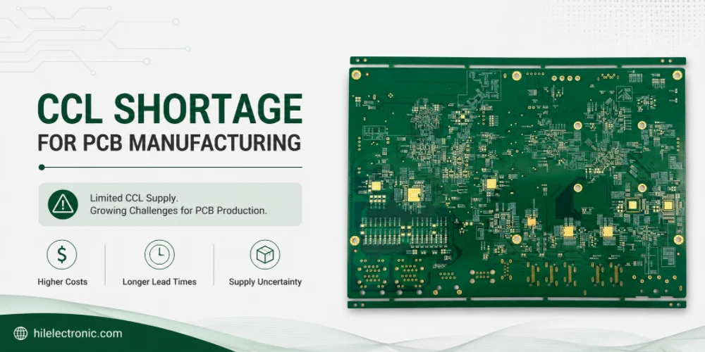
CCL Shortage for PCB Manufacturing
On this page Why Copper Clad Laminate Availability Matters...
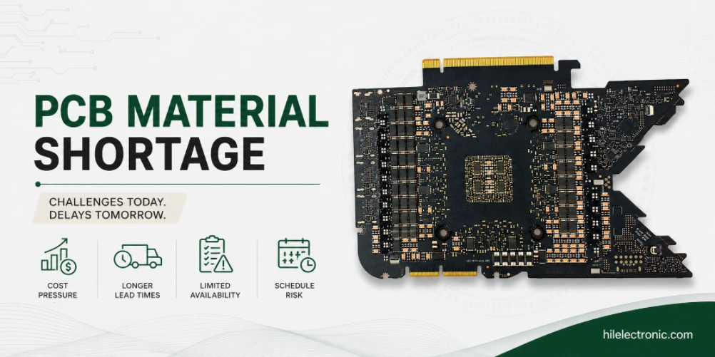
PCB Material Shortage Impact on Cost and Lead Time
On this page Why PCB Material Shortages Continue to Affect...
How to get a quote for PCBs
Let‘s run DFM/DFA analysis for you and get back to you with a report. You can upload your files securely through our website. We require the following information in order to give you a quote:
-
- Gerber, ODB++, or .pcb, spec.
- BOM list if you require assembly
- Quantity
- Turn time
In addition to PCB manufacturing, we offer a comprehensive range of electronic services, including PCB design, PCBA, and turnkey solutions. Whether you need help with prototyping, design verification, component sourcing, or mass production, we provide end-to-end support to ensure your project’s success.
For PCBA services, please provide your BOM (Bill of Materials) and any specific assembly instructions. We also offer DFM/DFA analysis to optimize your designs for manufacturability and assembly, ensuring a smooth production process.