
Electrical Schematic Diagram Services | PCB Manufacturing & PCB Assembly

What Is an Electrical Schematic Diagram?
An electrical schematic diagram is a graphical representation of an electrical circuit, illustrating the relationships between components using standardized symbols. It is not a physical layout but rather a logical flowchart that focuses on how components like resistors, capacitors, and ICs (Integrated Circuits) interact within a circuit.
Key Features of Electrical Schematics
-
- Component Symbols: Simplified, standardized icons represent various electrical elements.
- Connections: Lines and nodes illustrate how components are interconnected.
- Labels: Identifiers like “R1” for resistors or “C1” for capacitors help define components.
- Annotations: Additional notes may indicate values, ratings, or special instructions.
Electrical schematics serve as the blueprint for PCB design and manufacturing. Without a clear and accurate schematic, the journey from concept to a finished PCB can face delays, errors, and increased costs. Turn your Electrical Schematic Diagram into reliable PCBs and PCBAs with expert design, fabrication, and assembly services. Get support at every step.
The Role of Electrical Schematic Diagrams in PCB Design
Electrical schematic diagrams are a fundamental step in the PCB design process, acting as the backbone for converting a concept into a functional printed circuit board. These diagrams are not just technical drawings; they represent the logical flow and interconnection of electrical components, forming the foundation for creating a reliable and manufacturable PCB layout.
Why Electrical Schematic Diagrams Matter
Electrical schematic diagrams play a crucial role in ensuring the success of a PCB design. Here are the key reasons:
- Ensuring Design Accuracy
-
- A schematic translates the designer’s ideas into a clear, logical framework.
- It allows for the identification of potential design flaws, such as missing connections, incorrect pin assignments, or incompatible component values, before moving into the costly and time-intensive physical design stage.
-
- Facilitating PCB Layout Creation
-
- Modern PCB design software like Altium Designer, KiCad, or Eagle relies on the schematic to generate the PCB layout.
- By exporting netlists and component details from the schematic, these tools ensure the layout follows the intended electrical design, significantly reducing manual errors during component placement and trace routing.
-
- Optimizing for Manufacturing (DFM)
-
- A well-designed schematic integrates considerations for manufacturability, such as spacing between components, proper trace clearances, and ease of assembly.
- This reduces the likelihood of production delays or costly redesigns caused by layout errors.
-
- Simplifying Troubleshooting and Testing
-
- During prototyping or testing, the schematic serves as a roadmap for pinpointing and fixing issues. Technicians can trace faults in the PCB by comparing the physical board to its schematic.
- Post-production, the schematic becomes invaluable for product maintenance and repair, especially in complex designs with multiple interconnected layers.
-
- Professional Schematic Design as a Service
-
- Beyond creating PCB layouts from schematics, having professional expertise in schematic diagram design is essential for clients who need support in developing accurate and robust circuit designs from scratch. A well-crafted schematic is the cornerstone of a reliable PCB.
-
By ensuring the schematic is thorough, clear, and production-ready, designers can avoid many common pitfalls that arise later in the PCB lifecycle, ultimately saving time, reducing costs, and ensuring a high-quality final product.
At Highleap Electronic, we provide a comprehensive suite of one-stop electronic manufacturing services, including professional schematic diagram design, PCB layout, fabrication, PCB assembly, and testing. Whether you need support creating your schematic from the ground up or require full-scale manufacturing services, our team of experienced engineers and state-of-the-art production facilities ensure your project is handled with precision and efficiency.
From prototype development to mass production, we are committed to delivering solutions that meet your technical requirements, budget, and timeline. Contact us today to learn how we can help you turn your ideas into a fully realized product with unparalleled quality and performance!

12V charging protection indicator board schematic diagram
Best Practices for Creating Production-Ready Schematics
Creating a schematic that is production-ready is crucial for ensuring smooth PCB fabrication and assembly. A professional schematic minimizes errors, enhances manufacturability, and ensures your design intent is fully realized in the final product. Below are the best practices to follow when preparing a schematic for production.
1. Use Clear, Standardized Symbols
Adhering to international standards such as IEC, ANSI, or IPC for component symbols is essential. These standardized symbols provide consistency across the design, making it easier for engineers, manufacturers, and technicians to interpret the schematic. Avoid custom or non-standard symbols, as they can lead to misinterpretation. Furthermore, ensure all symbols are appropriately scaled and aligned to enhance the schematic’s readability.
2. Label Components and Connections Precisely
Every component in your schematic must be uniquely identified using reference designators (e.g., R1, C1, U1) that match the Bill of Materials (BOM). Clearly label net connections, pin numbers, and signal paths to ensure that the logical connections in the schematic match the physical routing on the PCB. Use hierarchical or modular block designs for complex circuits to group related components logically, and ensure signal flows are well-organized for ease of understanding.
3. Include Detailed Component Values and Specifications
Each component should include specific attributes, such as resistance (e.g., 10kΩ), capacitance (e.g., 100µF), voltage ratings (e.g., 16V), and tolerance levels. Providing this information reduces ambiguity during component sourcing and ensures compatibility with the intended design. For semiconductors, include additional parameters like part numbers, package types, and pinouts. Ensure the components you specify are readily available and compatible with your manufacturing partner’s capabilities to prevent delays during production.
4. Optimize Connections and Validate the Design
Simplify complex schematics by using net labels or bus connections for signals, power, and ground paths instead of drawing overly detailed wiring lines. This reduces visual clutter and improves readability. Before finalizing the schematic, use circuit simulation tools to validate functionality. Simulations can reveal critical issues such as incorrect voltage levels, signal integrity problems, and component interactions. Addressing these issues early prevents costly errors in the PCB layout or during physical testing.
By following these professional best practices, your schematic will not only ensure a smooth transition from design to production but also improve reliability, reduce manufacturing risks, and minimize production costs. A well-prepared schematic is a critical step toward achieving a high-quality end product.

How We Turn Your Schematics into High-Quality PCBs and PCBAs
As a professional PCB and PCBA manufacturer, we offer end-to-end solutions to bridge the gap between electrical design and physical production. Our streamlined process ensures that your schematic is not only accurately translated into a manufacturable PCB but also assembled into a reliable and functional product. Here’s a detailed look at how we achieve this:
1. Comprehensive Schematic Review
Before production begins, our team of skilled engineers conducts a thorough review of your schematic diagram to ensure it is optimized for seamless manufacturing and assembly.
-
- Error Detection: We examine the schematic for issues like incomplete connections, overlapping traces, incorrect pin assignments, or missing components.
- Design Validation: We cross-check your schematic with industry standards such as IPC, IEC, and ANSI, ensuring compliance and verifying that the design matches the intended functionality.
- Optimization for Manufacturing (DFM): We provide feedback on component placement, trace clearances, and signal integrity to reduce potential issues during production.
- Schematic Creation Support: If you don’t have a completed schematic, we can assist in designing it from scratch based on your project requirements.
2. Professional PCB Layout Design
Using the validated schematic, our layout engineers create a production-ready PCB design that ensures optimal performance and manufacturability.
-
- Custom Layouts: Whether it’s a single-layer board or a complex multi-layer design, we specialize in HDI (High-Density Interconnect) PCBs, high-frequency designs, and rigid-flex boards.
- Netlist Integration: We import your schematic’s netlist to ensure the PCB layout strictly adheres to your design intent.
- Signal Integrity and Power Analysis: To avoid issues like crosstalk or power delivery inefficiencies, we conduct detailed simulations and apply best practices during routing.
- Design Iteration: We collaborate with you throughout the process, allowing adjustments to ensure your PCB layout meets your exact requirements.
3. High-Precision PCB Fabrication
Our advanced fabrication process translates your PCB layout into a durable, high-quality circuit board.
-
- Cutting-Edge Capabilities: We produce single-layer, double-layer, and multi-layer PCBs, as well as high-frequency, HDI, and flexible PCBs.
- Material Options: We work with a wide range of materials, including FR4, aluminum, ceramic substrates, and PTFE laminates for RF applications.
- Tight Tolerances: Our advanced manufacturing ensures precise etching, drilling, and layer alignment to achieve high reliability.
- Environmental Compliance: All boards are manufactured to meet RoHS, REACH, and other environmental standards.
4. Component Procurement
Our global supply chain ensures the procurement of high-quality components that align with your schematic’s specifications.
-
- Cost Efficiency: By leveraging our established relationships with trusted suppliers, we ensure competitive pricing without compromising quality.
- Authenticity: We source only genuine, certified parts from reputable manufacturers to guarantee reliability.
- Inventory Management: If components in your BOM (Bill of Materials) are obsolete or unavailable, our team provides alternatives and ensures seamless integration with your design.
5. Seamless PCBA Assembly
Our state-of-the-art assembly lines guarantee flawless placement and soldering of components as outlined in your schematic.
-
- Advanced Technologies: We support SMT (Surface Mount Technology), THT (Through-Hole Technology), and mixed-technology assembly for a wide range of designs.
- Automated Precision: High-speed pick-and-place machines ensure micrometer-level accuracy for even the smallest components.
- Flexibility: From low-volume prototypes to high-volume production runs, we accommodate projects of all sizes.
- Specialized Requirements: We offer services such as conformal coating, BGA rework, and selective soldering for specialized applications.
6. Functional Testing and Quality Assurance
Quality is at the core of our process. After assembly, we conduct comprehensive testing to ensure your PCBAs meet your design’s specifications.
-
- ICT (In-Circuit Testing): Verifies continuity, component values, and electrical connections across the board.
- Functional Testing: We simulate real-world conditions to confirm the PCBAs function as intended.
- AOI (Automated Optical Inspection): Detects soldering defects, misaligned components, and other assembly issues.
- X-Ray Inspection: For complex designs, such as BGAs and multi-layer boards, we use X-rays to ensure there are no hidden defects.
7. Prototyping and Mass Production
We offer flexible production services, whether you need a few prototypes for testing or high-volume manufacturing for commercial deployment.
-
- Quick Turnaround Prototypes: For rapid testing and iterations, we provide expedited services while maintaining high-quality standards.
- Scalability: Once your design is finalized, we can seamlessly scale up to mass production.
- Design Refinements: Feedback from prototype testing can be incorporated into the final production batch for continuous improvement.
Why Partner With Us for Your PCB and PCBA Needs?
With years of experience and state-of-the-art facilities, we deliver a one-stop electronic manufacturing solution tailored to your project’s unique needs. Our services extend beyond just fabrication and assembly—we collaborate with you every step of the way, from schematic design to final product delivery.
Key Benefits of Choosing Us
-
- End-to-End Expertise: From schematic creation and PCB layout to final assembly and testing, we handle every aspect of your project.
- Cutting-Edge Technology: Our advanced machinery and tools ensure precision and reliability in every product we manufacture.
- Flexible Services: Whether you’re a startup developing prototypes or an established company scaling production, we provide customized solutions to meet your goals.
- Commitment to Quality: We adhere to stringent quality standards (e.g., ISO 9001, IPC Class 2/3, RoHS compliance) to guarantee exceptional performance and reliability.
- On-Time Delivery: With efficient processes and streamlined operations, we ensure your products are delivered on schedule.
At Highleap Electronic, we’re more than just a manufacturer—we’re your partner in bringing innovative ideas to life. Let us help you transform your schematic into a high-quality PCB or PCBA with our unmatched expertise and commitment to excellence.
Conclusion
As a professional PCB and PCBA service provider, we specialize in delivering end-to-end solutions. Whether you need assistance with schematic design, PCB layout, fabrication, component sourcing, assembly, or functional testing, we have the expertise, state-of-the-art facilities, and technical support to ensure your project’s success.
From concept to completion, we’re committed to bringing your designs to life with precision, quality, and efficiency. Contact us today to learn more about how our comprehensive services can help you turn your schematics into high-quality, reliable PCBs and PCBAs. Together, we can transform your ideas into innovative products that exceed expectations. Let us partner with you to achieve your goals, whether for prototypes or mass production.
FAQ
1. How do electrical schematic diagram services support PCB design?
Professional electrical schematic diagram services ensure your circuit is accurately documented before moving into PCB design. This step reduces errors, improves manufacturability, and helps generate a precise PCB layout that matches your intended functionality.
2. How to read electrical schematic diagrams for PCB projects?
To read electrical schematic diagrams, start by identifying symbols for resistors, capacitors, ICs, and power connections. Following the labeled nets and reference designators helps engineers understand how current flows, making it easier to transition into PCB layout and assembly.
3. Why are electrical schematics important for PCB manufacturing and assembly?
An electrical schematic for PCB design serves as the foundation for creating a reliable board. It ensures accurate component placement, netlist generation, and troubleshooting, making the entire PCB manufacturing and assembly process smoother and more cost-efficient.
4. Electrical schematic vs wiring diagram – what’s the difference?
An electrical schematic shows the logical flow of a circuit using standardized symbols, while a wiring diagram illustrates the physical connections and wiring locations. Schematics are essential for PCB design, while wiring diagrams are more common in installation and field work.
| Aspect | Electrical Schematic Diagram | Wiring Diagram |
|---|---|---|
| Purpose | Shows logical flow and function of a circuit | Shows physical connections and wiring placement |
| Symbols Used | Standardized electronic symbols (resistors, capacitors, ICs) | Realistic representations of wires and devices |
| Level of Detail | Focuses on how components interact logically | Focuses on where wires and components are located |
| Application | Essential for PCB design, simulation, and troubleshooting | Common in installation, repair, and field wiring |
| Audience | Engineers, PCB designers, technicians | Electricians, installers, maintenance teams |

Recommended Posts
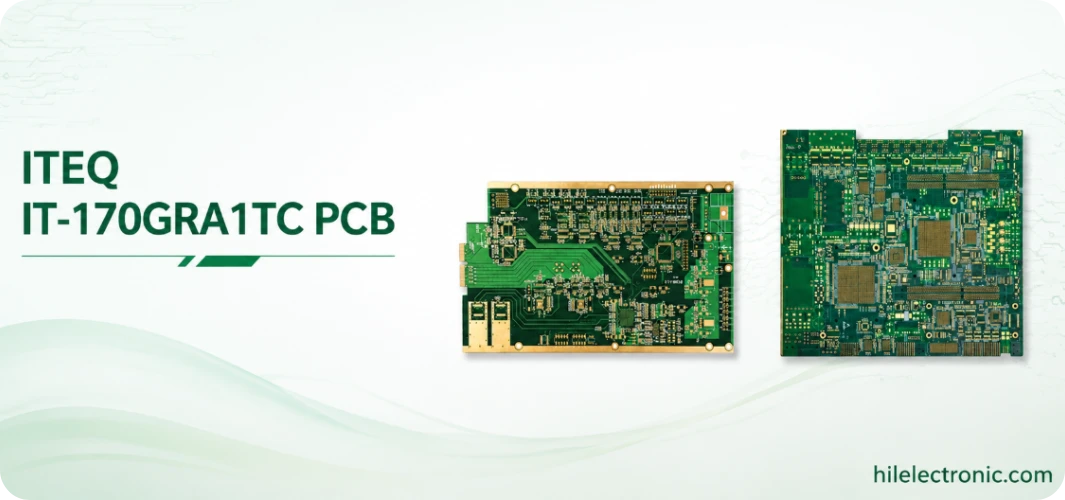
ITEQ IT-170GRA1TC PCB Manufacturer and Material Verification Service
Table of contentsFirst Verify What “IT-170GRA1TC”...
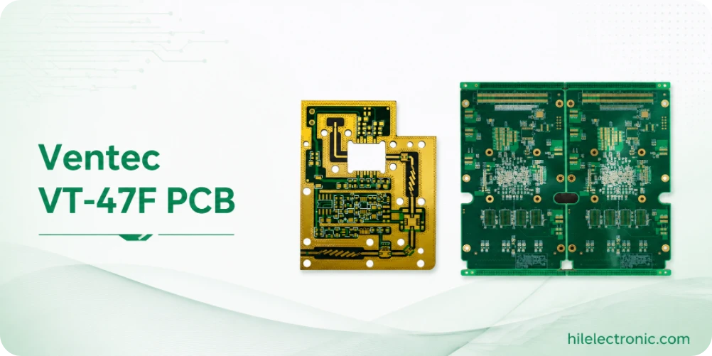
Ventec VT-47F PCB Material Verification Guide: VT-47 or VT-447?
Table of contentsIs VT-47F an Official Ventec PCB...
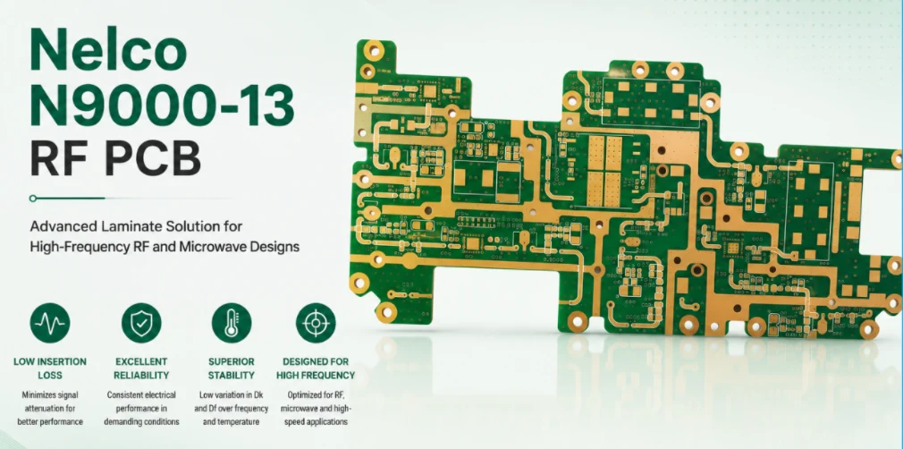
Nelco N9000-13 RF PCB Legacy Manufacturing and Replacement Service
Table of contentsCan Highleap Still Build a Nelco N9000-13...

RF Transceiver PCB Manufacturing and Assembly
Table of contentsRF Transceiver PCB Manufacturing and...
How to get a quote for PCBs
Let us run DFM/DFA analysis for you and get back to you with a report.
You can upload your files securely through our website.
We require the following information in order to give you a quote:
-
- Gerber, ODB++, or .pcb, spec.
- BOM list if you require assembly
- Quantity
- Turn time
In addition to PCB manufacturing, we offer a comprehensive range of electronic services, including PCB design, PCBA (Printed Circuit Board Assembly), and turnkey solutions. Whether you need help with prototyping, design verification, component sourcing, or mass production, we provide end-to-end support to ensure your project’s success. For PCBA services, please provide your BOM (Bill of Materials) and any specific assembly instructions. We also offer DFM/DFA analysis to optimize your designs for manufacturability and assembly, ensuring a smooth production process.