
Glass Core PCB for Advanced Packaging

A glass core PCB is an advanced package substrate that uses a thin glass sheet instead of the organic resin core found in conventional flip-chip BGA substrates. The main reason for using glass is not novelty, but performance: glass offers a coefficient of thermal expansion much closer to silicon, much lower warpage at large package sizes, and better dimensional stability for fine-pitch interconnects. These properties make glass core substrates increasingly relevant for AI accelerators, high-performance CPUs, chiplet packages, and other advanced semiconductor assemblies where organic substrates approach their mechanical and routing limits. The broader material and process background sits within glass PCB technology.
Request a Glass Core PCB Quote
Table of Contents
What Is a Glass Core PCB?
A glass core PCB is a package substrate in which the central core layer is made from glass rather than an organic laminate such as BT resin or modified FR-4. In advanced semiconductor packaging, this core acts as the rigid structural backbone of the substrate, defining flatness, thickness stability, and vertical interconnect geometry. Instead of conventional drilled vias, the glass core uses through-glass vias to route signals and power through the substrate thickness.
The glass itself is not an active electrical layer. Its role is structural and dimensional. Copper redistribution layers and dielectric build-up layers are formed above and below the glass core, while the glass provides the stable base needed for fine-pitch die attach and large-format package construction. In practical terms, a glass core PCB is not the same as a standard rigid glass circuit board used in general electronics; it is specifically aimed at advanced IC package substrate applications where silicon compatibility and warpage control are critical.
This is why glass core PCB is increasingly discussed alongside next-generation processor packaging. As package sizes grow and bump pitch continues to shrink, the core material becomes a limiting factor, and glass offers a different performance ceiling than organic substrate technology.
Why Glass Core PCB Is Replacing Organic Package Substrates
Organic package substrates have supported semiconductor packaging for decades, but advanced AI and HPC packages are now pushing beyond the reliable limits of organic core behavior. The most important issue is thermal-mechanical mismatch. Organic substrate cores typically have a coefficient of thermal expansion far above silicon, which creates stress at the die-to-substrate interface during reflow and thermal cycling. As bump pitch becomes finer, that stress becomes more difficult to absorb without solder fatigue and joint reliability problems.
Glass core PCB addresses this by bringing the substrate CTE much closer to silicon. That reduces relative displacement during temperature change and helps maintain solder joint reliability across large die footprints. The second major advantage is warpage control. Large organic substrates tend to bow during assembly because of asymmetrical thermal expansion across the stack-up. At advanced package sizes, that warpage can create open joints or inconsistent bump attachment. Glass has much better dimensional stability, allowing flatter panels and more uniform interconnect formation.
A third driver is interconnect density. Organic cores depend on mechanically drilled via structures with larger minimum dimensions, while glass cores can support much finer vertical interconnect formation. For modern chiplet integration, where routing density and package size increase together, that combination of lower warpage, better CTE match, and finer via capability is the main reason glass core PCB is moving into commercial adoption.
Glass Core PCB vs Organic Core vs Glass Interposer
Glass core PCB sits between organic package substrates and silicon or glass interposer solutions in the performance-cost landscape. Compared with an organic core substrate, glass offers lower warpage, lower moisture absorption, better dimensional stability, and a much closer thermal match to silicon. Compared with a silicon interposer, glass core substrates can support larger panel-scale manufacturing and lower overall cost, while still enabling much finer wiring and via density than organic materials.
| Property | Glass Core PCB | Organic Core Substrate | Glass / Silicon Interposer |
|---|---|---|---|
| Core material | Glass | BT resin / FR-4 derivative | Glass or silicon redistribution layer platform |
| CTE match to silicon | Very close | Poorer | Best |
| Warpage control | Excellent | Limited at large size | Excellent |
| Via density | High | Moderate | Very high |
| Manufacturing format | Panel-level | Panel-level | Often wafer-level |
| Relative cost | Moderate | Lowest | Highest |
The key distinction between a glass core PCB and a glass interposer is functional position in the package. A glass core substrate is the package substrate itself, including build-up layers and the board-level connection interface. A glass interposer is a passive redistribution element placed between dies and substrate for ultra-high-density routing. If your focus is interposer architecture rather than substrate construction, the role of glass interposer PCB is different.
Glass Core PCB Structure and Build-Up Design
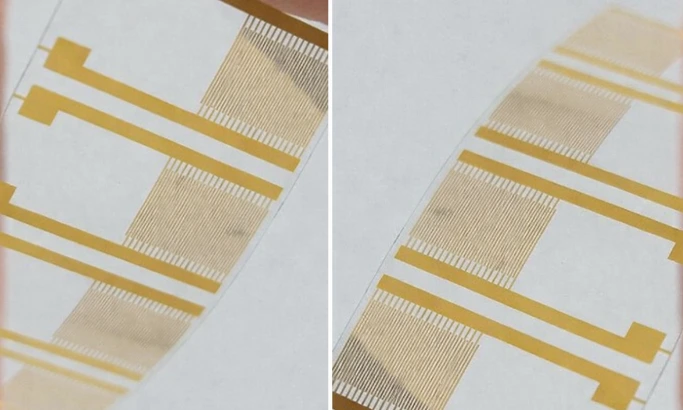
A typical glass core PCB is built around a thin glass sheet, usually in the range of 0.1 mm to 0.3 mm, with through-glass vias formed through the core and copper-filled for vertical interconnection. On both sides of the glass, build-up dielectric and copper redistribution layers are added to create the package routing structure. The top side typically supports fine-pitch die attach, while the bottom side provides the solder ball or package-level interconnect interface.
The most important stack-up rule is symmetry. Glass itself is dimensionally stable, but the complete substrate can still warp if the top and bottom build-up layers are not balanced. Copper density, dielectric thickness, and layer count should be closely matched on both sides so that thermal stress remains balanced during reflow and underfill cure. For this reason, glass core substrate design is not only about choosing glass as a material; it is also about controlling the full build-up architecture around that core.
Material selection matters as well. Borosilicate glass is commonly preferred because it provides a favorable combination of thermal stability, mechanical properties, and process compatibility. The differences between available glass PCB substrate materials matter when choosing a core for package development.
TGV and Warpage Design Considerations
Through-glass via design is one of the core engineering topics in glass core PCB development. TGV diameter, pitch, aspect ratio, copper filling quality, capture pad size, and edge keepout all directly affect manufacturability and reliability. Compared with standard PCB via design, TGV structures require tighter control because the surrounding material is brittle glass rather than an organic laminate. Via placement too close to the substrate edge or excessive local stress concentration can create crack sensitivity during processing or singulation.
For that reason, TGV design is closely tied to warpage and stress management. Even though glass dramatically reduces core-level deformation compared with organic materials, the finished substrate still experiences stress from copper imbalance, die attach, underfill cure, and temperature cycling. Good glass core PCB design therefore combines fine TGV layout with balanced copper distribution, matched build-up layers, and package-level mechanical modeling.
In practical terms, the design goal is not just to make a via conductive. It is to make the entire core-and-build-up structure stable enough for fine-pitch flip-chip bonding across the full package area. The process details behind through-glass via formation directly affect that result.
Applications and Glass Core PCB FAQ
Glass core PCB is being adopted where conventional package substrates no longer provide enough flatness, thermal matching, or routing density. The strongest demand comes from AI accelerators, high-performance CPUs, and chiplet-based package architectures with large body size and very fine bump pitch. These packages need a substrate that remains flat through assembly while supporting high I/O density and reliable die attachment. Glass core also has growing relevance in high-frequency and RF packaging, where dielectric stability and dimensional precision matter at advanced operating frequencies. In those cases, the electrical behavior of high-frequency glass PCB structures becomes part of the package design discussion.
What is the main advantage of a glass core PCB?
The main advantage is the combination of low warpage and CTE compatibility with silicon. This makes glass core substrates more suitable than organic cores for large, fine-pitch semiconductor packages.
Is a glass core PCB the same as a glass interposer?
No. A glass core PCB is the package substrate itself, while an interposer is a separate redistribution layer positioned between dies and substrate.
Why is glass core PCB important for AI and chiplet packages?
Because those packages combine large substrate size, high I/O count, and fine bump pitch. Organic materials struggle to maintain flatness and reliability under those conditions, while glass performs better.
Does glass core PCB replace silicon interposers?
Not in every design. Glass core usually occupies a middle ground between lower-cost organic substrates and higher-performance interposer solutions.
Is glass core PCB already a production technology?
It is moving from development into early production for advanced packaging programs, especially where large substrate size and fine interconnect density are required. Project requirements can be sent directly through the quote page.

Recommended Posts
Rogers TMM3 PCB Manufacturer for Mechanical RF Modules
TMM3 is selected when an RF circuit must behave as part of...
Rogers RO3003 PCB Manufacturer for Automotive Radar and mmWave Modules
A 77 GHz radar board is purchased as a working sensor...
Rogers RO4835T PCB Manufacturer for Thin-Core RF Multilayer Boards
RO4835T is useful when the RF layer must move inside the...
Rogers RO4003C PCB Manufacturer for RF and Hybrid Multilayer Boards
RO4003C is often the point where an RF project stops...
How to get a quote for PCBs
Let us run DFM/DFA analysis for you and get back to you with a report.
You can upload your files securely through our website.
We require the following information in order to give you a quote:
-
- Gerber, ODB++, or .pcb, spec.
- BOM list if you require assembly
- Quantity
- Turn time
In addition to PCB manufacturing, we offer a comprehensive range of electronic services, including PCB design, PCBA (Printed Circuit Board Assembly), and turnkey solutions. Whether you need help with prototyping, design verification, component sourcing, or mass production, we provide end-to-end support to ensure your project’s success. For PCBA services, please provide your BOM (Bill of Materials) and any specific assembly instructions. We also offer DFM/DFA analysis to optimize your designs for manufacturability and assembly, ensuring a smooth production process.