
Glass Interposer PCB vs Silicon Interposer

A glass interposer is a passive redistribution substrate placed between semiconductor dies and the package substrate below them. Its main job is to redistribute fine-pitch die connections into a routing format that the next level of packaging can handle, while also carrying die-to-die signals, power, and ground across a compact area. In practice, glass interposers are attracting attention because they offer a middle position between silicon interposers and organic interposers: finer routing and better dimensional stability than organic materials, but lower cost potential and larger panel-format manufacturing than wafer-limited silicon. For the broader material and platform context, see the glass PCB overview.
Request a Glass Interposer Quote
Quick answer
Glass interposers are used when a package needs finer redistribution than organic substrates can economically provide, but does not need the extreme density and cost of a silicon interposer. They are especially relevant for chiplet packages, AI accelerator assemblies, RF SiP, and photonic-electronic co-packaging.
Table of Contents
What Is a Glass Interposer and What Does It Do?
In advanced semiconductor packaging, an interposer is a redistribution layer positioned between the dies above and the package substrate below. A glass interposer uses glass as its base substrate and combines three essential functions: horizontal signal redistribution through fine wiring on the surface, vertical transfer through the thickness of the substrate, and pitch translation between very fine die bumps and the coarser interconnect structure underneath.
This means a glass interposer is not the same thing as a complete package substrate. It does not replace the whole bottom package. Instead, it sits between the dies and the package substrate, helping route dense signals in a space where ordinary package wiring becomes too coarse. The package substrate below still handles the broader fan-out and board-level connection, while the interposer manages the dense local interconnect problem directly under and between the dies.
A typical glass interposer structure includes a thin glass core, through-glass vias for vertical connection, and redistribution layers on one or both sides. Because the glass itself is electrically insulating and dimensionally stable, it provides a good platform for fine wiring, pitch translation, and co-packaging structures that would be difficult to realize on standard organic materials.
Glass Interposer vs Silicon Interposer vs Organic Interposer
The reason glass interposer technology matters is that it sits in a very useful middle ground. Silicon interposers offer the finest routing density, but they are expensive and constrained by wafer-scale manufacturing. Organic interposers are lower cost and easier to scale, but their routing density and dimensional stability are more limited. Glass interposers fill the gap for packages that need more density than organic can comfortably provide, but do not need the full cost and complexity of silicon.
| Comparison point | Glass interposer | Silicon interposer | Organic interposer |
|---|---|---|---|
| Routing density | Fine | Very fine | Moderate |
| CTE match to silicon | Good | Best | Weak |
| Manufacturing format | Panel scale | Wafer scale | Panel scale |
| Optical transparency | Yes | No | No |
| Relative cost | Moderate | Highest | Lowest |
From a packaging decision perspective, silicon interposer is usually selected when the design absolutely requires the finest redistribution density available. Organic interposer is preferred when cost dominates and the routing density requirement remains moderate. Glass interposer becomes attractive when the package needs better dimensional stability, finer routing, or optical functionality without moving fully into silicon-interposer cost territory.
Glass Interposer Design: TGV, RDL, Stack-Up, and Warpage Control
Glass interposer design is the most important part of the topic because the value of the interposer is determined less by the material name and more by how the structure is engineered. In real projects, a glass interposer is not judged only by whether it uses glass. It is judged by whether its through-substrate interconnect, redistribution layers, stack symmetry, and package interaction can support the target die size, bump pitch, signal count, and assembly process.
1. Glass core thickness and role
The glass core is usually kept thin because the interposer is a redistribution structure, not a large mechanical board. The glass needs to be thick enough to maintain dimensional stability during processing and assembly, but thin enough to support the intended via geometry and package profile. In this role, the glass behaves differently from a full substrate platform such as glass core PCB, where the glass forms the central structural backbone of the package substrate itself.
2. Through-glass vias as the vertical backbone
Through-glass vias are critical because they connect the die-facing routing side to the package-facing side. In glass interposers, these vias usually have tighter spacing, smaller dimensions, and stricter fill requirements than in more general glass circuit work. Solid fill is commonly favored because the interposer has to support dense redistribution and stable vertical performance rather than just occasional top-to-bottom transitions. The detailed process logic behind this vertical interconnect is closely related to through-glass via fabrication.
3. Redistribution layer design
The redistribution layer, or RDL, is where the interposer actually performs its pitch-translation function. On the top side, the RDL receives fine-pitch die connections. On the bottom side, it transitions those signals toward the package substrate. When multiple dies share one interposer, the same RDL network also routes die-to-die connections laterally across the surface. This means the routing strategy must consider signal escape, path length, reference structure, local density, and how the interposer interacts with the organic substrate underneath.
In practice, interposer RDL design is not just “finer PCB routing.” It is closer to packaging redistribution, where local density, symmetry, and layer interaction are tightly coupled to assembly and warpage behavior. A layout that looks electrically efficient may still be structurally poor if it creates copper imbalance or unsupported stress concentrations in the interposer stack.
4. Stack-up symmetry and warpage management
Warpage is one of the central engineering risks in glass interposer design because fine bump pitch leaves very little margin for assembly distortion. If the redistribution structure is not balanced, cooling from assembly temperature can create enough curvature to cause bump opens, uneven contact, or yield loss. The most common contributors are copper imbalance between the two sides, mismatched dielectric build-up, underfill behavior, and interaction with the package substrate below.
For that reason, interposer stacks are usually designed with symmetry in mind. The top and bottom redistribution structures need to be considered together, not independently. Copper density balance, layer count, and process order all influence the final flatness of the interposer. This is one of the main reasons glass is attractive: its lower CTE and good dimensional stability help control package deformation better than organic alternatives in dense package environments.
5. Signal, power, and thermal planning
Although the interposer is passive, it still has to carry three different system functions: signal redistribution, power distribution, and thermal interaction with the rest of the package. These do not always push the design in the same direction. Dense lateral signal routing may compete with the need for power delivery paths or ground continuity. Similarly, bump layout and die placement may create local thermal concentration zones. Good interposer design therefore requires coordination across electrical, mechanical, and packaging objectives rather than optimizing only one of them.
This is why a glass interposer should be treated as a package design problem, not only a fine-line routing problem. The correct via pattern, RDL stack, and build-up arrangement are determined by the whole package architecture, including die count, die spacing, substrate below, and assembly method.

Where Glass Interposers Are Used in 2.5D, 3D, and Co-Packaged Optics
Glass interposers are most often discussed in the context of advanced packaging, but the application types are not all the same. The interposer can serve very different roles depending on whether the package is 2.5D, 3D, or photonic-electronic.
2.5D chiplet packaging
In 2.5D packages, multiple dies sit side by side on the interposer, and the interposer handles the dense lateral routing between them. This is one of the clearest use cases for glass interposer technology because it demands fine redistribution, stable geometry, and scalable substrate area.
3D packaging support structures
In 3D configurations, the interposer may serve as the base redistribution layer supporting a more vertically integrated stack. The importance here is not only routing density but also mechanical stability and vertical interconnect reliability within a more tightly coupled package.
Photonic-electronic co-packaging
One of the most distinctive advantages of glass interposer technology is its optical transparency. This property opens a design space that neither silicon interposers nor organic substrates can support in the same way. In photonic–electronic co-packaged systems, optical and electrical functions can be integrated on the same substrate platform, enabling more compact and efficient architectures for high-bandwidth communication and sensing applications.
These use cases also show why glass interposers cannot be evaluated purely through simple cost comparisons. In some packaging solutions, glass may be selected because it is less expensive than silicon. In other cases, it is chosen for its unique capabilities, such as optical access, larger substrate formats, or different material characteristics. In these situations, glass functions not just as a lower-cost alternative but as a substrate that enables design options unavailable with other materials.
Glass Interposer FAQ and Project Planning
What is the difference between a glass interposer and a glass core substrate?
A glass interposer is a passive redistribution layer inserted between the dies and the package substrate. A glass core substrate is the full package substrate structure that sits below the die or interposer and ultimately connects to the board-level package interface.
When is glass interposer better than silicon interposer?
Glass interposer is typically more attractive when the package needs finer redistribution than organic materials can provide, but does not need the most extreme density available from silicon interposer. It also becomes more interesting where panel-scale economics or optical functionality matter.
What information is needed to start a glass interposer project?
The project normally starts with die size, die count, bump map, target footprint, signal count, data rate, power requirements, and the package structure below the interposer. Those inputs determine the interposer routing density, via strategy, and stack-up direction.
Can glass interposers be assembled with standard flip-chip methods?
They can be integrated into standard advanced assembly flows, but the tooling and support approach must reflect the brittle substrate behavior of glass. Assembly planning is usually reviewed alongside the broader package process path described in glass PCB manufacturing.
How should a project be quoted?
A useful quotation usually begins with the package architecture rather than with a bare dimensions-only request. If you already have die information, bump map, footprint target, or interconnect constraints, submit them through the quote page so the glass interposer can be reviewed against the actual package requirements.

Recommended Posts
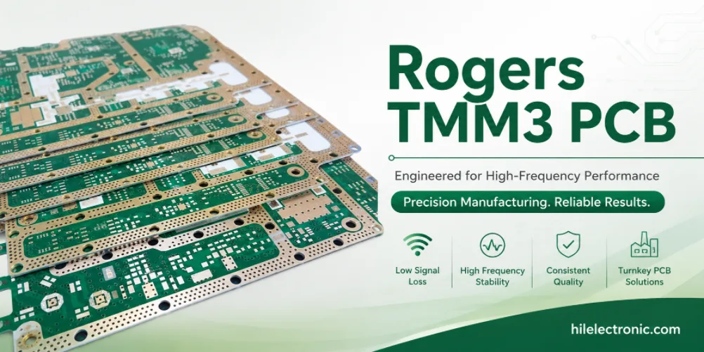
Rogers TMM3 PCB Manufacturer for Mechanical RF Modules
TMM3 is selected when an RF circuit must behave as part of...
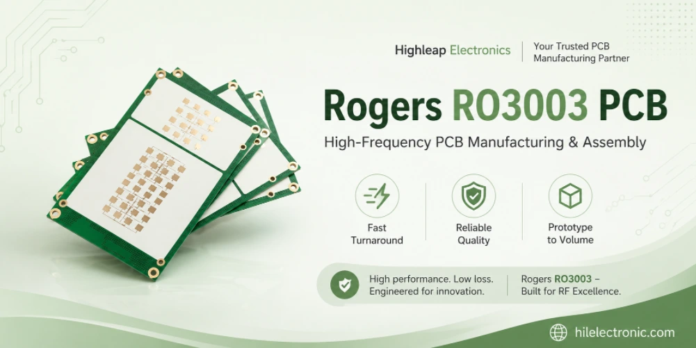
Rogers RO3003 PCB Manufacturer for Automotive Radar and mmWave Modules
A 77 GHz radar board is purchased as a working sensor...
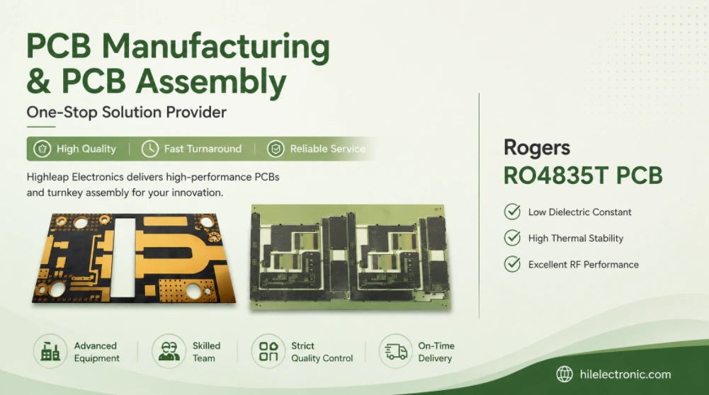
Rogers RO4835T PCB Manufacturer for Thin-Core RF Multilayer Boards
RO4835T is useful when the RF layer must move inside the...
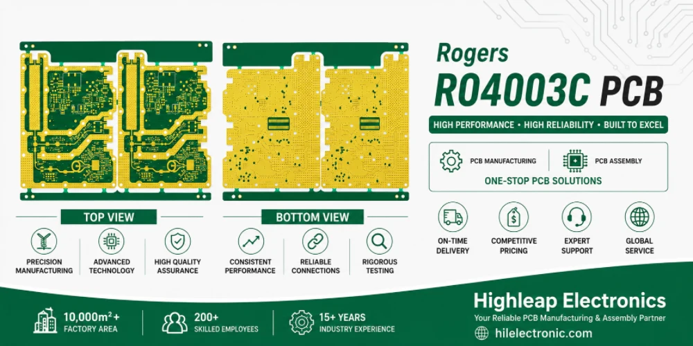
Rogers RO4003C PCB Manufacturer for RF and Hybrid Multilayer Boards
RO4003C is often the point where an RF project stops...
How to get a quote for PCBs
Let us run DFM/DFA analysis for you and get back to you with a report.
You can upload your files securely through our website.
We require the following information in order to give you a quote:
-
- Gerber, ODB++, or .pcb, spec.
- BOM list if you require assembly
- Quantity
- Turn time
In addition to PCB manufacturing, we offer a comprehensive range of electronic services, including PCB design, PCBA (Printed Circuit Board Assembly), and turnkey solutions. Whether you need help with prototyping, design verification, component sourcing, or mass production, we provide end-to-end support to ensure your project’s success. For PCBA services, please provide your BOM (Bill of Materials) and any specific assembly instructions. We also offer DFM/DFA analysis to optimize your designs for manufacturability and assembly, ensuring a smooth production process.