
Through Glass Via in Glass PCB Design

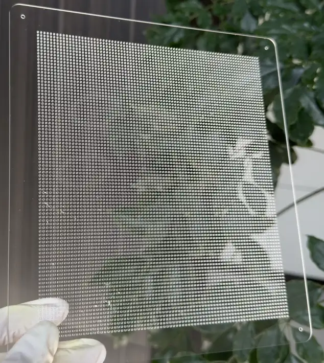
A through-glass via(TGV) is a vertical electrical connection formed through a glass substrate. In glass PCB design, it allows signals, power, ground, or heat to move through the thickness of the glass so the substrate can support routing between surfaces, layers, and functional regions. This makes through-glass vias an important design feature in glass PCB layouts, glass core structures, interposer-style routing, and RF circuits where flatness, dimensional stability, and controlled interconnection all matter. As part of glass PCB design, a through-glass via is not only a manufacturing feature, but also a routing and integration feature that shapes how the whole substrate is used.
Quick Answer
In glass PCB design, a through-glass via is the structure that enables vertical routing through a glass substrate. It connects conductors on opposite sides of the glass and supports denser layouts, build-up integration, ground transitions, power transfer, and thermal paths in glass core, interposer, RF, and specialty glass circuit applications.
Table of Contents
What Through-Glass Via Means in Glass PCB Design
In glass PCB design, a through-glass via is the vertical interconnect that links conductor features on the top and bottom sides of a glass substrate. Without it, the glass can only support much simpler surface routing. Once through-glass vias are introduced, the design can begin to use both surfaces of the substrate in a coordinated way, and the glass becomes part of a more complete circuit architecture instead of acting only as a rigid support.
This is why a through-glass via should not be understood as just a hole through glass. It is a design structure with electrical, mechanical, and process implications. The opening in the glass, the metal inside it, the pad geometry around it, and the routing connected to it all work together.
- Electrical role: connects signals, ground, power, or thermal paths through the glass body
- Mechanical role: must be compatible with a brittle, rigid substrate
- Routing role: lets both sides of the glass share circuit functions
- Integration role: supports more complex layouts than single-surface glass routing
Routing Role of Through-Glass Vias in Glass PCBs
The main routing role of a through-glass via is to move electrical paths through the substrate so the design is not limited to one surface. In a glass PCB, routing area is often more constrained than in an ordinary multilayer organic board because the design may need to preserve optical space, manage conductor density carefully, or support different functions on opposite sides of the substrate. A through-glass via helps solve that problem by adding vertical routing to the layout strategy.
This becomes especially useful when the top and bottom sides of the glass are assigned different jobs. One side may be used for fine-pitch signal routing, while the opposite side may be used for ground reference, power distribution, shielding structures, thermal paths, or larger interconnect pads.
| Glass PCB side | Typical role | Why the through-glass via matters |
|---|---|---|
| Top side | Fine-pitch signals / active routing | Moves routing to the opposite side when surface space is limited |
| Bottom side | Ground, power, pads, shielding, thermal structures | Links different electrical functions across the substrate thickness |
As routing density increases, via location, pitch, and pad transition begin to affect the whole organization of the circuit. This is one reason through-glass via planning is closely connected to glass PCB manufacturing, where via formation, conductor patterning, and surface utilization have to work together.
Why Glass Changes Via Design Logic
A through-glass via cannot be treated the same way as a plated through-hole in an FR-4 board because glass changes the design logic. Organic laminates are drilled and plated in a mature multilayer PCB process, and their vias are usually handled as standard stack-up features. Glass is different. It is rigid, brittle, highly dimensionally stable, and less tolerant of edge damage or uncontrolled crack initiation.
That means the via is not only an electrical transition but also a local mechanical event in the substrate. Via placement, edge spacing, local metal loading, and thickness relationship all need more attention than they do in ordinary FR-4 layouts.
| Topic | FR-4 via thinking | Glass via thinking |
|---|---|---|
| Substrate behavior | More forgiving mechanically | Brittle and crack-sensitive |
| Via placement | Mostly routing-driven | Routing + stress + edge control |
| Metal balance | Important | More closely tied to flatness and local stress |
Metallization and Build-Up Integration
Metallization is central to through-glass via performance because the opening in the glass only becomes useful after it is converted into a stable conductive structure. In design terms, metallization affects more than electrical continuity. It also affects adhesion, resistance, process compatibility, surface flatness around the via, and how well the vertical interconnect joins the conductor system on both sides of the substrate.
For that reason, metallization should be treated as part of the design architecture rather than only as a downstream fabrication step.
- Opening formation: the via path is created in the glass with controlled geometry
- Surface preparation: the glass surface is conditioned for reliable metal adhesion
- Seed and conductive build-up: the via becomes a usable vertical conductor
- Integration with routing: the via joins pads, traces, and build-up features on both sides
This becomes more demanding when the via is part of a build-up substrate rather than a simple two-sided glass circuit. That is why through-glass via design is closely related to glass core PCB structures, where vertical interconnect, build-up balance, and substrate stability have to be considered together.
Design Considerations for Glass Core, Interposer, and RF Structures
The design considerations for a through-glass via depend strongly on the type of glass structure being built. The same via concept can play very different roles depending on whether the substrate is intended for package integration, interposer routing, or RF performance.
Glass core structures
In glass core substrates, the via is usually part of a denser package-style interconnect system. Routing efficiency, build-up symmetry, vertical transition quality, and substrate flatness all matter together.
Interposer structures
In interposer-style layouts, the via works as part of a redistribution architecture where conductor density and layout precision are central to the function of the substrate. This is the kind of environment where glass interposer PCB layouts rely on through-glass vias as part of the routing network rather than as isolated connections.
RF structures
In RF and microwave structures, the via may be part of grounding, shielding, reference transitions, or controlled signal movement through the glass body. In these designs, via geometry cannot be separated from pad structure, return path, conductor arrangement, and surrounding dielectric behavior. This is why through-glass via planning is often considered together with high-frequency glass PCB requirements.
Applications and FAQ
Through-glass vias support glass PCB applications by allowing the substrate to carry more than one circuit function at the same time. In some layouts, they connect signal features between the two surfaces of a rigid glass board. In others, they help separate signal, ground, and power functions across different sides of the substrate. In denser package-related structures, they support vertical transitions inside a compact interconnect network.
They are also useful where electrical routing has to be combined with other substrate-level requirements. Some transparent or semi-transparent structures need conductor placement to be managed carefully while preserving interconnection through the substrate. Some thermal or lighting-related designs need vertical conductive paths that support both routing and heat movement. This is why through-glass vias also appear in certain LED glass PCB structures.
FAQ
What is the main function of a through-glass via in glass PCB design?
Its main function is vertical routing through the glass substrate, allowing top and bottom conductor systems to work together.
Why is a through-glass via different from a standard PCB via?
Because the via is formed in a brittle glass substrate rather than in an organic laminate, so routing, stress, and metallization all need different design logic.
Where are through-glass vias most commonly used?
They are commonly used in glass core structures, interposer-style layouts, RF circuits, and some LED or thermal glass designs.
As glass-based circuit technology continues to expand, through-glass vias remain one of the design features that makes that expansion possible. They allow glass to function not only as a rigid or transparent substrate, but as part of a more capable interconnect system for advanced packaging, RF routing, and specialized electronic integration. Project requirements can be submitted directly through the quote page.

Recommended Posts

TUC TU-872 SLK PCB for High-Speed FR-4 Cost Control
TUC TU-872 SLK occupies a commercially useful middle...

Shengyi S1000-2M PCB for Thick Multilayer Reliability
Shengyi S1000-2M is a high-Tg, low-CTE FR-4.0 laminate for...
Isola P25N PCB for No-Flow Bonding and Cavity Builds
Isola P25N is a polyimide UL HB No-Flo® specialty prepreg....
ITEQ IT-88GMW PCB for 77 GHz Radar Modules
A 76–81 GHz automotive radar PCB is an electromagnetic...
How to get a quote for PCBs
Let us run DFM/DFA analysis for you and get back to you with a report.
You can upload your files securely through our website.
We require the following information in order to give you a quote:
-
- Gerber, ODB++, or .pcb, spec.
- BOM list if you require assembly
- Quantity
- Turn time
In addition to PCB manufacturing, we offer a comprehensive range of electronic services, including PCB design, PCBA (Printed Circuit Board Assembly), and turnkey solutions. Whether you need help with prototyping, design verification, component sourcing, or mass production, we provide end-to-end support to ensure your project’s success. For PCBA services, please provide your BOM (Bill of Materials) and any specific assembly instructions. We also offer DFM/DFA analysis to optimize your designs for manufacturability and assembly, ensuring a smooth production process.