
LED Glass PCB Manufacturing for Transparent Lighting

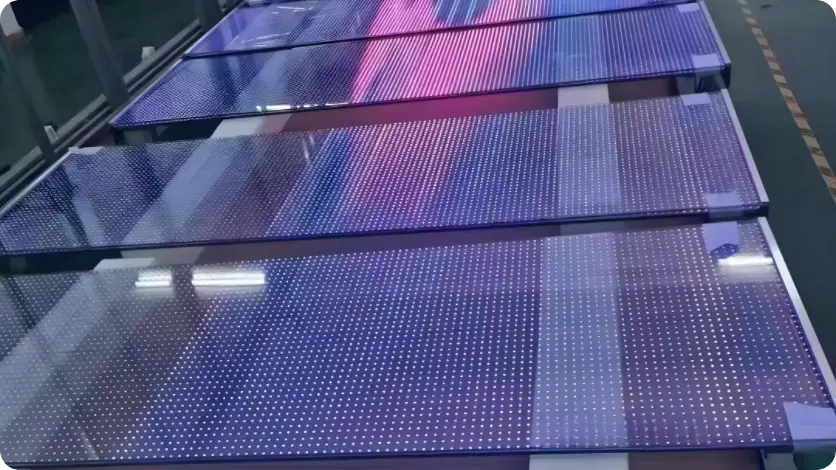
LED glass PCB manufacturing for transparent lighting combines glass substrate processing, conductor patterning, LED mounting, and assembly control into one production flow. At Highleap Electronics, these projects are reviewed not only as circuit boards, but as transparent lighting structures where visibility, conductor layout, LED pitch, current distribution, and assembly quality all affect the final product. This is why transparent LED panels, glass lighting walls, and decorative lighting systems require a different engineering and production approach from standard PCB fabrication.
Request an LED Glass PCB Manufacturing Quote
What Highleap reviews before LED glass PCB production
- Panel size, glass thickness, and target visible area
- LED pitch, package size, and expected lighting effect
- Conductor structure, power-entry location, and perimeter routing plan
- Whether the project needs bare board fabrication only or full LED assembly
Table of Contents
What LED Glass PCB Manufacturing Includes
LED glass PCB manufacturing is the process of building lighting circuits directly on glass substrates so the finished panel can provide illumination while remaining transparent or semi-transparent. In these products, the glass is not only a mechanical support. It is also part of the visible lighting surface, which means the manufacturing process has to control both electrical function and visual quality.
At Highleap, LED glass PCB manufacturing usually involves four linked stages: glass selection, conductor formation, LED pad and routing definition, and final assembly or testing. The exact process route depends on whether the product is a transparent LED display panel, a decorative lighting wall, a smart-glass lighting structure, or another glass-based lighting system.
Compared with ordinary LED boards, the manufacturing goal is different. A standard LED PCB is mainly judged by current delivery, solderability, and thermal behavior. An LED glass PCB must also be judged by visible appearance. Routing patterns, LED spacing, conductor coverage, and residue control all affect whether the finished panel still looks like glass when the LEDs are off. In broader glass PCB technology, this is one of the clearest cases where fabrication quality and product appearance are directly connected.
Glass and Conductor Choices for Transparent Lighting
The first production decision is the glass substrate. Indoor decorative lighting and retail display panels may use soda-lime or borosilicate depending on panel size, cost target, and service conditions. Outdoor installations, automotive-related lighting, or more thermally demanding products more often move toward borosilicate because it offers stronger stability under temperature change and environmental stress. For projects where substrate behavior is critical, borosilicate glass substrates are often the more suitable option.
The second major decision is the conductor system. Transparent lighting products still need practical current delivery, so the conductor cannot be chosen by appearance alone. In most LED glass PCB projects, metallic conductor structures remain the practical solution because they support real LED current and provide reliable solderable pads. The manufacturing challenge is to control conductor visibility while keeping the routing electrically stable.
| Project type | Typical glass choice | Typical conductor choice | Main reason |
|---|---|---|---|
| Indoor transparent LED panel | Soda-lime or borosilicate | Fine metallic conductor network | Balances transparency, cost, and practical LED drive routing |
| Glass lighting wall | Borosilicate or thicker architectural glass | Perimeter-fed metallic routing | Supports larger panel formats and stable lighting effect |
| Decorative lighting system | Soda-lime or borosilicate | Low-visibility metallic routing | Preserves appearance while supporting moderate LED load |
| Hybrid transparent function | Application-specific | Hybrid conductor structure | Used only when current demand and transparency need to be mixed |
At Highleap, glass and conductor selection are reviewed together rather than independently. A transparent LED panel, a decorative glass partition, and a lighting wall may all fall under LED glass PCB manufacturing, but they do not use the same glass thickness, routing pattern, or pad structure.
How Highleap Plans LED Glass PCB Manufacturing for Transparent Panels
This is the most important part of the process, because transparent lighting products do not succeed through material choice alone. The manufacturing plan has to balance transparency, LED pitch, current delivery, pad design, and thermal behavior in one coordinated structure. A panel that looks visually clean but cannot deliver current evenly will show brightness variation. A panel that handles current well but ignores visibility will stop looking like transparent lighting glass. At Highleap, this balance is reviewed before production release rather than after the layout is already fixed.
Visible zone and support zone are separated early
For most transparent lighting products, Highleap first checks whether the design clearly separates the viewing area from the support area. The viewing area should contain only the conductor and LED structures required for the intended lighting effect. The support area, usually at the perimeter, is where denser bus routing, connectors, and stronger electrical features should be placed. This is one of the most effective ways to preserve transparency without weakening the electrical structure.
LED pitch is reviewed against both appearance and manufacturability
Smaller pitch improves image density or lighting uniformity, but it also increases pad count, package coverage, conductor density, and local heat load. Wider pitch improves transparency and keeps the panel cleaner, but it changes the visual effect. Highleap reviews LED pitch not only as a display decision, but also as a fabrication, routing, and assembly decision.
Current distribution is reviewed at panel level
LEDs are current-driven devices, so the panel has to be evaluated as one electrical system rather than as isolated LED pads. In larger transparent panels, heavy current paths should be moved toward perimeter or hidden regions whenever possible, while the visible field uses lighter routing. This keeps the active optical zone cleaner while maintaining usable brightness and electrical stability across the panel.
Pad design follows the LED package, not only the transparency target
The LED body already blocks the glass at its mounting point, which means the pad area under the package can be made stronger than the routing area between LED positions. Highleap uses this principle in project review because it allows more reliable soldering and better local thermal spreading without creating unnecessary visual penalty in the clear area.
Thermal planning is tied to the real product structure
Thermal behavior is checked with the final product in mind, not only as a bare board exercise. Frame design, mounting method, panel size, and heat flow all affect how the glass lighting product performs after assembly. For projects that require more structural coordination, this review often overlaps with glass PCB design, because visible area definition, routing strategy, and manufacturability are tightly linked.
Keep the viewing zone visually light, move heavier current paths toward the perimeter, and treat LED landing areas as functional mounting zones rather than trying to make every conductor feature equally transparent.
LED Assembly on Glass Substrates
LED assembly on glass substrates uses standard SMT principles, but it requires more careful panel support, alignment control, and optical cleanliness than ordinary FR-4 assembly. Since the finished circuit remains visible, any placement deviation, solder excess, or residue can affect both product reliability and appearance.
At Highleap, LED glass PCB assembly review typically focuses on solder paste volume, LED placement accuracy, support method during reflow, and post-assembly cleanliness. Thin or large glass panels often require dedicated support fixtures so the substrate remains stable during transport and heating. Optical inspection is also more demanding because the finished product is judged not only by solder joint quality but also by transparency and visible cleanliness.
| Assembly stage | Why Highleap reviews it closely |
|---|---|
| Paste deposition | Controls visible excess solder and bridge risk |
| LED placement | Affects both electrical reliability and visible alignment |
| Reflow support | Prevents handling and transport stress on glass |
| Cleaning and inspection | Residue and optical defects are more visible on transparent panels |
Projects that require finished product assembly are best reviewed together with surface-mount assembly services so the fabrication route, support fixture, and inspection standard are defined before production begins.
Typical Products: Transparent LED Panels, Glass Lighting Walls, and Decorative Lighting Systems
LED glass PCB manufacturing is most often used for products where the glass itself remains part of the visible design. Transparent LED panels are used in retail and commercial displays where the panel must still be seen through when the content is off. Glass lighting walls are used in hospitality, architecture, and interior installations where the panel becomes an illuminated surface. Decorative lighting systems use glass-based circuits when the product must combine lighting effect with a premium visible finish instead of hiding the electronics behind another layer.
| Product category | Main production priority | Typical challenge |
|---|---|---|
| Transparent LED panel | Maintain high off-state transparency | Balancing LED density and conductor visibility |
| Glass lighting wall | Create a large illuminated surface with clean appearance | Managing heat and current across broad panels |
| Decorative glass lighting system | Preserve design quality while integrating LEDs | Keeping support structures visually discreet |
| Retail window lighting | Support visibility through the glass when off | Power delivery across large transparent spans |
Can LED glass PCB manufacturing replace ordinary LED board production in every lighting product?
No. If the product does not need transparency, visible-area aesthetics, or direct integration into glass, a conventional LED board is usually simpler and more cost-effective.
Can Highleap support both fabrication and LED assembly?
Yes. Depending on the project, Highleap can review the job as glass circuit fabrication only or as a combined fabrication-and-assembly project, which is often more suitable for transparent lighting products.
What should be submitted for quotation?
Submit the panel size, glass preference, LED pitch, target brightness, visible-area definition, and whether you need bare board fabrication only or full LED assembly. If you already have a concept or layout, use the quote form so Highleap can review the project against actual manufacturing, assembly, and optical requirements.

Recommended Posts
Low CTE FR-4 PCB Manufacturing for Through-Hole Reliability
Low CTE FR-4 PCB manufacturing is used when a circuit...
Halogen Free FR-4 PCB Manufacturing for Controlled Material Builds
Halogen free FR-4 PCB manufacturing is used when a product...
FR408HR PCB Material for High-Reliability Multilayer Boards
FR408HR PCB material is selected when a multilayer board...

Nelco N4000-13EP PCB Manufacturer for High-Reliability Multilayer Boards
Nelco N4000-13EP PCB manufacturing is used for...
How to get a quote for PCBs
Let us run DFM/DFA analysis for you and get back to you with a report.
You can upload your files securely through our website.
We require the following information in order to give you a quote:
-
- Gerber, ODB++, or .pcb, spec.
- BOM list if you require assembly
- Quantity
- Turn time
In addition to PCB manufacturing, we offer a comprehensive range of electronic services, including PCB design, PCBA (Printed Circuit Board Assembly), and turnkey solutions. Whether you need help with prototyping, design verification, component sourcing, or mass production, we provide end-to-end support to ensure your project’s success. For PCBA services, please provide your BOM (Bill of Materials) and any specific assembly instructions. We also offer DFM/DFA analysis to optimize your designs for manufacturability and assembly, ensuring a smooth production process.