
Glass PCB Design for Transparent, Rigid, and Package-Style Circuits

Glass PCB design is the engineering process of turning a glass substrate into a workable circuit structure while balancing electrical performance, mechanical reliability, manufacturability, and, in some projects, optical requirements. Unlike standard FR-4 layout work, glass-based design cannot be treated as a simple material substitution. The substrate is rigid, brittle, dimensionally stable, and often used for applications that need finer routing, transparent areas, tighter flatness control, or package-style interconnection. That means glass PCB design starts with structure definition, not just copper routing. Designers usually need to decide early how the glass will be used, what kind of interconnect is required, where stress will concentrate, and how fabrication and assembly will affect the finished board. For the broader technology background, see the glass PCB overview.
Request a Glass PCB Design Review
Before starting a glass PCB design
- Define whether the board is rigid, transparent, package-style, or substrate-through interconnected
- Choose the substrate family before finalizing routing density or stack-up assumptions
- Identify whether the design includes optical zones, fine interconnect, or assembly constraints
- Review manufacturability early, because glass layout decisions are tightly linked to process capability
Table of Contents
What Glass PCB Design Means
Glass PCB design is more than routing copper on a non-standard substrate. It includes selecting the right glass type, defining how the circuit will use the substrate, planning conductor architecture, controlling stress and edge conditions, and matching the design to the intended fabrication route. In some projects, the glass mainly provides flatness, chemical stability, or transparency. In others, it is part of a denser interconnect structure that depends on fine routing, redistribution layers, or vertical interconnection through the substrate.
That is why glass PCB design usually begins with structure category rather than with line width alone. A transparent glass circuit, a rigid glass sensor board, a glass core package substrate, and a glass interposer-related layout do not follow the same design priorities even though all of them fall under the same broad material family. If the wrong structure assumption is made at the start, later routing and assembly decisions often become much harder to correct.
Material choice is part of design, not a separate purchasing decision. Different glass PCB substrate options change the electrical, thermal, optical, and mechanical behavior of the board. Borosilicate, aluminosilicate, fused silica, and soda-lime glass are not interchangeable in layout terms, because each one changes how the board should be routed, handled, and assembled.

How Glass PCB Design Differs from Standard PCB Design
The main difference is that glass imposes structural constraints much earlier than FR-4 does. Standard PCB layout often starts with electrical connectivity and then checks manufacturability afterward. In glass PCB design, the order is usually reversed or at least simultaneous. Mechanical behavior, edge distance, substrate thickness, via strategy, transparent area control, and assembly method have to be considered while the layout is still taking shape.
Glass is rigid and dimensionally stable, which is helpful for precision routing and package-style structures, but it is also brittle. That changes how designers treat corners, cutouts, unsupported regions, and transitions between fine conductors and heavier metalized areas. A layout that looks electrically simple in CAD can still be weak in handling or difficult to manufacture if edge stress, local density, or substrate-through features are not planned carefully.
Another difference is that glass is often chosen because the board must do something beyond ordinary PCB routing. Transparent circuits need controlled visible areas. Package-style designs may need tighter flatness and better CTE behavior. Boards using substrate-through interconnect need their routing and pad structure planned around through-glass via requirements from the beginning. In other words, glass PCB design is usually function-led rather than material-led.
Core Design Rules for Glass PCB Layout and Structure
This is the most important part of glass PCB design, because the success of the project depends less on the idea of “using glass” and more on whether the structure is laid out in a way that glass can actually support. Good glass PCB design is a coordinated balance between substrate behavior, conductor density, interconnect strategy, optical area, and assembly method.
Start with the structural role of the substrate
The first design question is what the glass is doing in the product. If the glass is mainly providing transparency, the routing and component placement have to protect visible area. If it is providing flatness and stability for package-style routing, the stack-up and conductor balance matter more. If it is part of a sensing or optical platform, clear regions, coatings, and alignment features may matter as much as the copper itself. This structural role determines the rest of the layout logic.
Keep edge and cutout design conservative
Glass is more sensitive to edge damage and crack propagation than ordinary laminate boards. For that reason, traces, pads, vias, and copper-heavy regions should not be pushed too aggressively toward edges or internal cutouts. Corner shape, slot geometry, and unsupported narrow sections all influence handling reliability. A design can be electrically correct and still fragile if the outline is not coordinated with the mechanical behavior of glass.
Plan copper density, not just net connectivity
On glass, local metal distribution affects more than current capacity. It also influences stress balance, flatness behavior, visual appearance in transparent designs, and the transition between fine features and reinforced connection zones. Dense copper on one side and sparse copper on the other can create imbalance in build-up or package-style structures. In transparent designs, copper density also affects how the board looks through the substrate, which means routing decisions become part of the optical design as well.
Match interconnect style to the board function
Not every glass PCB needs substrate-through interconnect, but if it does, that decision has to be made early. Routing strategy changes when signals or power must move vertically through the glass. Pad capture, keepout, layer assignment, and return-path planning all depend on that choice. In denser package-related structures, this can overlap with glass core PCB design or even glass interposer planning, where the substrate is part of a more advanced redistribution architecture.
Separate visible area from functional support area
In transparent glass circuits, one of the most effective design strategies is to separate the active viewing or optical zone from the support zone. The support zone can carry denser routing, reinforced interconnects, connectors, and larger components, while the optical zone is kept as open and visually clean as possible. This is also one reason transparent designs need to be reviewed together with transparent PCB requirements rather than treated as normal rigid boards made from a clear material.
Design the stack-up and routing as one system
On glass, conductor routing, pad geometry, substrate thickness, and surface finish should not be treated as separate steps. They influence each other directly. A thinner substrate may improve one part of the design but make handling and assembly harder. A denser routing pattern may solve an electrical problem but create local stress or visual interference. A package-style build may need symmetry and balance rather than simply more routing layers. Strong glass PCB design comes from making these decisions together instead of optimizing each one in isolation.
Reserve room for real assembly constraints
Glass boards are often used in designs where the bare board is only half the challenge. Fixtures, placement support, thermal profile, connector loading, and handling during assembly all affect whether the final product is reliable. This is especially important in thin boards, transparent layouts, and structures with fine interconnect or delicate edges. Good design leaves enough mechanical margin for the real assembly process instead of only the idealized board drawing.
Designing for Manufacturability and Assembly
Glass PCB design should be reviewed through a manufacturability lens before prototype release. In practice, DFM for glass goes beyond trace width and spacing. It usually includes substrate fit, board shape, edge condition, interconnect strategy, assembly readiness, and whether the design belongs to the right process category in the first place. A layout that looks reasonable on screen may still need changes once substrate handling, metallization, singulation, or fixture support are considered.
Designers should check whether the stack-up matches the selected substrate, whether optical and mechanical zones are clearly defined, whether transitions into connectors or reinforced areas are robust, and whether any through-substrate features are placed realistically. Projects that move into fabrication too early often discover that the problem was not electrical connectivity, but unsupported glass geometry, poor balance, or an assembly assumption that did not fit the material.
This is why glass PCB design should be coordinated with glass PCB manufacturing before the layout is locked. On many projects, the best DFM outcome is not a minor note about spacing. It is a structural adjustment that makes the board easier to fabricate, easier to assemble, and more likely to survive early prototypes without redesign.
Typical Glass PCB Design Scenarios
Glass PCB design appears in several recurring scenarios, and each one pushes the layout in a different direction. In rigid sensor or industrial boards, the value often comes from stability, cleanliness, and environmental resistance. In transparent products, the challenge is balancing circuitry with visible area. In package-style designs, the substrate becomes part of a denser interconnect system with tighter flatness and routing requirements. In LED or lighting-related structures, thermal behavior, visible zones, and conductor placement may all matter at the same time. Some of these project types also intersect with LED glass PCB design requirements.
When should a design move to glass instead of FR-4?
Glass usually becomes worth considering when the design needs transparency, substrate stability, package-style flatness, special interconnect geometry, or environmental behavior that ordinary laminate boards do not support as well. If the project does not need those advantages, FR-4 may still be the more practical choice.
Does every glass PCB need through-glass vias?
No. Some glass boards are surface-routed only. Substrate-through interconnect is needed only when the structure or package requires vertical electrical transfer through the glass.
What is the best way to start a glass PCB project?
The best starting point is to define the structure clearly before the routing is finalized: substrate family, board role, optical zones, vertical interconnect need, and assembly method. If you already have a layout or concept, submit it through the quote page so the design can be reviewed against actual material and process constraints.

Recommended Posts
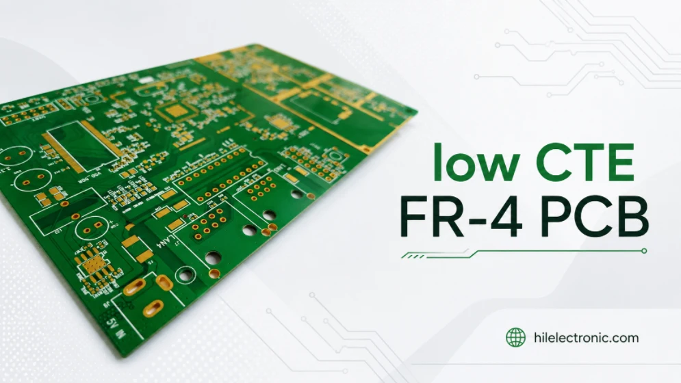
Low CTE FR-4 PCB Manufacturing for Through-Hole Reliability
Low CTE FR-4 PCB manufacturing is used when a circuit...
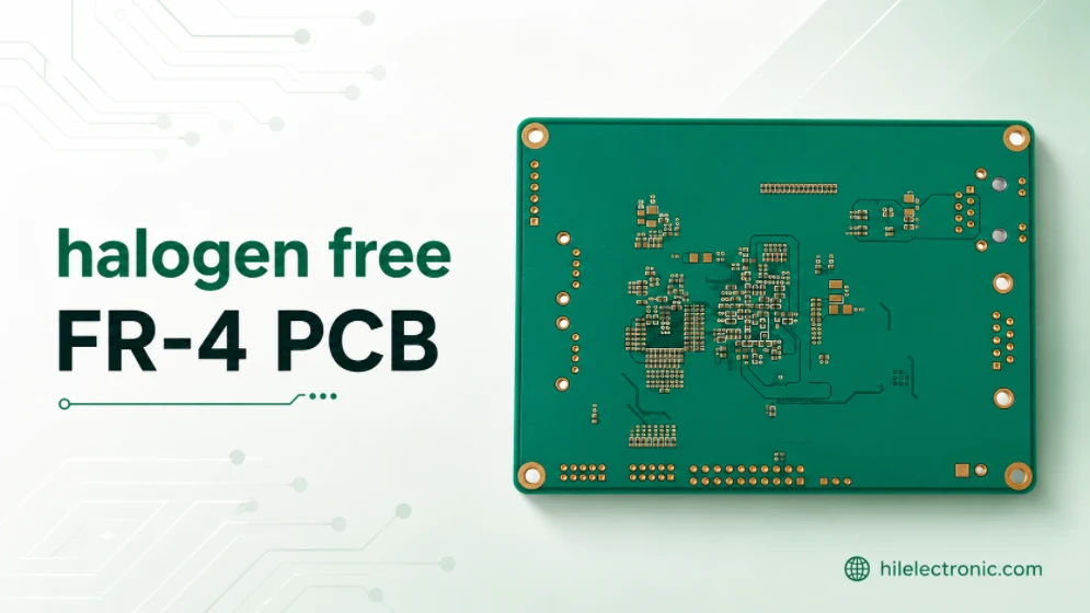
Halogen Free FR-4 PCB Manufacturing for Controlled Material Builds
Halogen free FR-4 PCB manufacturing is used when a product...
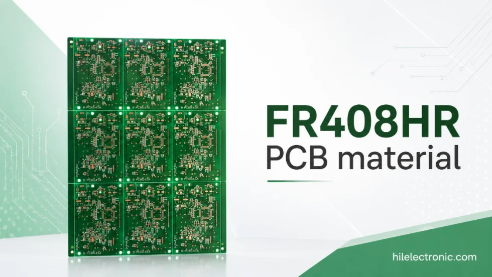
FR408HR PCB Material for High-Reliability Multilayer Boards
FR408HR PCB material is selected when a multilayer board...

Nelco N4000-13EP PCB Manufacturer for High-Reliability Multilayer Boards
Nelco N4000-13EP PCB manufacturing is used for...
How to get a quote for PCBs
Let us run DFM/DFA analysis for you and get back to you with a report.
You can upload your files securely through our website.
We require the following information in order to give you a quote:
-
- Gerber, ODB++, or .pcb, spec.
- BOM list if you require assembly
- Quantity
- Turn time
In addition to PCB manufacturing, we offer a comprehensive range of electronic services, including PCB design, PCBA (Printed Circuit Board Assembly), and turnkey solutions. Whether you need help with prototyping, design verification, component sourcing, or mass production, we provide end-to-end support to ensure your project’s success. For PCBA services, please provide your BOM (Bill of Materials) and any specific assembly instructions. We also offer DFM/DFA analysis to optimize your designs for manufacturability and assembly, ensuring a smooth production process.