
Back to blog
HASL vs ENIG: Which Surface Finish Should You Choose?
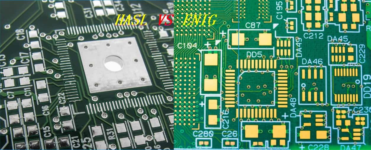
Selecting the most suitable surface finish for printed circuit boards (PCBs) is a critical decision in electronic design and manufacturing. Among the numerous options available, two prominent choices are Hot Air Solder Leveling (HASL) and Electroless Nickel Immersion Gold (ENIG). Both methods aim to protect the copper traces on PCBs from oxidation while ensuring good solderability. This article delves deep into the differences between HASL and ENIG, offering an extensive analysis of their advantages, disadvantages, and applications, along with a detailed comparison to aid engineers and designers in making informed decisions for their specific projects.
Understanding HASL (Hot Air Solder Leveling)

HASL Process Overview
HASL, an acronym for “hot air solder leveling,” is a widely employed PCB surface finishing technique. This process involves coating the exposed copper traces and pads on a PCB with a layer of liquid solder, which is then evenly distributed using hot air knives. The result is a solder finish that safeguards the copper from oxidation and ensures good solderability.
Two Primary Types of HASL Finishes
a. Lead-based HASL: Utilizes a tin-lead solder alloy containing tin and lead, offering excellent shelf life and solderability but raising environmental and health concerns.
b. Lead-free HASL: Employs lead-free solder alloys composed of tin combined with silver, copper, or bismuth as a substitute for lead. Compliant with RoHS standards but potentially more susceptible to oxidation and requiring higher processing temperatures.
Advantages of HASL
a. Simple Process: HASL is a straightforward process compared to other surface finish methods, making it accessible to a wide range of PCB manufacturers.
b. Low Cost: HASL is a cost-effective surface finish solution, ideal for budget-conscious projects.
c. Availability: It is widely accessible and commonly offered by PCB manufacturers.
d. Visual Inspectability: The HASL finish can be visually inspected for quality and coverage.
e. Suitability for Through-Hole Components: HASL’s robust coating makes it well-suited for through-hole component assembly, withstanding the soldering process.
Disadvantages of HASL
a. Surface Smoothness: The solder layer can exhibit unevenness, posing challenges for Surface Mount Technology (SMT) and fine-pitch components.
b. Dimensional Tolerances: HASL may not be suitable for very thin or thick PCBs due to limitations in achieving precise thickness control.
c. Thermal Stress: High temperatures during processing can potentially damage PCBs, making it less suitable for sensitive applications.
d. Hole Tolerance: HASL may struggle to meet tight tolerances on plated holes, affecting the overall PCB quality.
e. Wire Bonding: The HASL finish is not compatible with wire bonding applications, limiting its use in certain electronic designs.
Applications of HASL
HASL is well-suited for various applications, including:
a. Low-budget Electronics: Its affordability makes HASL suitable for mass-producing budget consumer devices.
b. Prototyping: The quick turnaround time and decent durability of HASL make it a preferred choice for prototyping PCBs.
c. Non-critical Longevity: Products with shorter lifespans benefit from HASL’s sufficient lifespan without incurring additional costs.
d. Education and Hobbyists: The accessibility and ease of use make HASL a suitable choice for educational or hobbyist PCB fabrication.
Understanding ENIG (Electroless Nickel Immersion Gold)

ENIG Process Overview
ENIG, short for Electroless Nickel Immersion Gold, is a widely adopted PCB surface finish known for its durability and long-lasting performance. This process involves the deposition of a thin gold layer over a nickel electroless layer, providing exceptional protection against oxidation.
Advantages of ENIG
a. Lead-free: ENIG does not contain lead, making it compliant with RoHS standards and environmentally friendly.
b. High Conductivity: The gold layer ensures excellent electrical conductivity, enhancing overall PCB performance.
c. Flat Surface: ENIG offers a flat and smooth surface, making it highly suitable for fine-pitch components and Surface Mount Technology (SMT), ensuring precise component placement.
d. Durability: ENIG-coated boards exhibit robust resistance to environmental stresses and physical wear over extended periods.
e. Good Shelf Life: PCBs with ENIG surface finish maintain their solderability for a longer duration, offering extended shelf life.
Disadvantages of ENIG
a. Expensive: The cost of materials and processing for ENIG is higher compared to HASL, which can be a limiting factor for cost-sensitive projects.
b. Difficult Rework: Removing and replacing components on ENIG-finished PCBs is more challenging than with HASL finish due to the complex nature of the finish.
c. Signal Loss: The thin gold layer in ENIG can cause slight signal loss at high frequencies, which may impact certain high-frequency applications.
d. Complex Process: The ENIG deposition method is more intricate and time-consuming than HASL, requiring specialized equipment and expertise.
e. Black Pad Risk: Weak gold-nickel bonding in ENIG can potentially lead to “black pad” defects, affecting PCB reliability.
Applications of ENIG
ENIG is often the preferred PCB surface finish in applications characterized by:
a. Fine-pitch Components: ENIG’s smooth and flat finish accommodates the placement of tiny, delicate parts with tight spacing, making it ideal for high-density designs.
b. Advanced Soldering: Technologies like lead-free soldering benefit from ENIG’s exceptional solderability and flat surface.
c. Long-term Reliability: When PCBs must function consistently over extended periods without degradation, ENIG provides the necessary durability.
d. Harsh Environments: The corrosion protection offered by ENIG makes it suitable for mechanically and thermally demanding conditions, ensuring long-term performance.
Differences Between HASL vs ENIG
To aid in the decision-making process, the following table provides a detailed comparison between HASL and ENIG in various parameters:
| Parameter | HASL | ENIG |
|---|---|---|
| Metal Coating | Tin-lead or tin-silver-copper | Nickel and gold |
| Plating Thickness | Thicker solder layer | Thinner gold layer |
| Adhesion to Copper | Good due to metallurgical bond | Good due to nickel barrier layer |
| Heat Stress | High risk of damage | Low risk of warping |
| Electrical Abilities | Lower | Higher due to gold |
| Flatness | Can be uneven | Smooth finish |
| Soldering | Good for manual soldering | Compatible with advanced techniques |
| Component Compatibility | Suits through-hole and SMT, not suitable for fine-pitch | Allows all component types including fine-pitch |
| Use Conditions | Not advised for harsh environments | Withstands harsh environments |
| Cost | Cost-effective, simple process | More expensive due to gold immersion process |
| Shelf Life | Lower, prone to oxidation | Longer due to gold preventing oxidation |
| Eco-Friendly | Lead variant not eco-friendly | Environmentally safe |
HASL vs. ENIG: Selecting the Right Surface Finish
When making the critical decision between HASL and ENIG surface finishes for your PCB project, it’s essential to consider the specific requirements of your application:
- HASL is a cost-effective option with a simple process, making it suitable for projects where cost savings and availability are paramount. It is also a good choice for applications with through-hole components, prototyping, and non-critical longevity.
- ENIG offers a smooth, thin gold coating over a nickel layer, providing excellent oxidation resistance and a long shelf life. It excels in applications requiring fine-pitch components, wire bonding, superior solderability, and reliability in harsh environmental conditions.
Before making a selection, carefully assess factors such as the desired shelf life, solderability, component compatibility, environmental resilience, and budget constraints to ensure the chosen surface finish aligns with your PCB design objectives.
HASL vs ENIG: Key Differences and How to Choose the Best PCB Surface Finish
When comparing HASL vs ENIG, one of the key considerations is the specific needs of your project, particularly in terms of surface smoothness and component compatibility. HASL, while cost-effective, can result in uneven surfaces due to the nature of the hot air solder leveling process. This unevenness can pose challenges, especially when working with fine-pitch components or high-density surface mount technology (SMT). ENIG, on the other hand, offers a much smoother, flat surface that excels in handling fine-pitch components, making it the preferred option for high-precision applications. The gold layer in ENIG not only provides excellent solderability but also enhances the reliability and longevity of the PCB, ensuring that the board can endure repeated thermal cycles and harsh environmental conditions.
In the debate of HASL vs ENIG, another crucial factor is the difference in their environmental impact and compliance with industry standards. Lead-based HASL, although effective in terms of solderability, raises significant environmental concerns due to the presence of lead. For industries and regions adhering to RoHS (Restriction of Hazardous Substances) regulations, lead-free HASL or ENIG becomes mandatory. ENIG, being lead-free by nature and offering superior corrosion resistance, aligns well with environmental standards while providing better long-term performance. For applications that prioritize environmental sustainability and compliance, such as medical devices or automotive electronics, ENIG is often the more appropriate choice compared to HASL.
Common Misconceptions About HASL and ENIG
Choosing between HASL and ENIG can be confusing, and certain misconceptions may lead to suboptimal decisions:
- HASL Is Always Cheaper: While HASL has lower upfront costs, its uneven surface can increase assembly defects in fine-pitch applications, leading to higher rework costs.
- ENIG Is Immune to All Defects: Despite its durability, ENIG is susceptible to “black pad” issues if not manufactured under strict process controls.
- One Size Fits All: Each project has unique requirements. HASL may be ideal for prototypes, but ENIG is necessary for high-frequency or high-reliability applications.
Decision-Making Guide
- For budget-limited projects or through-hole components, HASL is sufficient.
- For high-density boards, fine-pitch components, or harsh environments, ENIG is the better choice.
- Consider hybrid finishes or consulting a manufacturer to tailor the finish to your application.
Hidden Costs in Choosing Between HASL and ENIG
While upfront costs often drive decision-making, hidden costs throughout the manufacturing and lifecycle of the PCB can have a significant impact:
- Rework and Scrap Rates:
- HASL: The uneven surface can cause solder bridging or misaligned components, increasing rework rates.
- ENIG: Although it offers better assembly precision, improper gold-nickel bonding can lead to black pad defects, resulting in costly replacements.
- Equipment Investment:
- Switching to lead-free HASL or ENIG may require manufacturers to upgrade their production lines, adding initial capital expenses.
- Long-Term Reliability:
- ENIG’s longer shelf life and environmental resistance reduce maintenance and replacement costs in the long run, making it more cost-effective for products with extended lifespans.
Conclusion
In the world of PCB manufacturing, the choice between HASL and ENIG surface finishes can significantly impact the performance, reliability, and cost-effectiveness of electronic devices. This comprehensive exploration of the two surface finish methods has provided engineers and designers with the knowledge needed to make informed decisions for their specific projects. Whether prioritizing cost-efficiency or demanding the highest levels of performance and reliability, the choice between HASL and ENIG ultimately hinges on the unique requirements of the application at hand.

Recommended Posts

Exploring PCB Surface Treatment: The Significance of ENIG and DIG
PCB Surface Treatment:ENIG PCB With the ever-evolving...

How PCB Dry Film Plays a Key Role in Enhancing PCB Reliability
PCB dry film pressing equipmentWhat is PCB Dry Film? Dry...
High-Quality Rigid PCB Circuit Board Fabrication Services
HDI Rigid PCBWhat are rigid PCB and flexible PCB? In the...

PCB Mounting Holes: Understanding Counterbore and Countersink
Counterbore and Countersink--PCB Hole TypesPCBs are...
How to get a quote for PCBs
Let us run DFM/DFA analysis for you and get back to you with a report.
You can upload your files securely through our website.
We require the following information in order to give you a quote:
-
- Gerber, ODB++, or .pcb, spec.
- BOM list if you require assembly
- Quantity
- Turn time
In addition to PCB manufacturing, we offer a comprehensive range of electronic services, including PCB design, PCBA (Printed Circuit Board Assembly), and turnkey solutions. Whether you need help with prototyping, design verification, component sourcing, or mass production, we provide end-to-end support to ensure your project’s success. For PCBA services, please provide your BOM (Bill of Materials) and any specific assembly instructions. We also offer DFM/DFA analysis to optimize your designs for manufacturability and assembly, ensuring a smooth production process.