
Back to blog
The Most Common Applications for PCBs by Industry

In today’s increasingly high-tech world, printed circuit boards (PCBs) serve as the foundation for the majority of electronic devices we use on a daily basis. From the smartphone in your pocket to the appliances in your kitchen, PCBs enable electronics to function through their purposeful and intricate design.
The global PCB market was valued at $72.6 billion in 2022 and is projected to reach $107.4 billion by 2030, exhibiting a CAGR of 4.3% from 2023 to 2030 (ResearchAndMarkets, 2022). This growth reflects PCBs’ expanding applications across industries along with continued innovation in PCB technology itself.
PCBs have evolved tremendously over the past several decades, becoming progressively smaller, more reliable, and able to facilitate more complex functionalities. This article provides an overview of what PCBs are, their expanding applications across industries, key design considerations, and a look toward the future of PCB capabilities.
What Are PCBs and How Do They Work?
A PCB serves as the foundation onto which electronics components are mounted and interconnected to create functional circuits. PCBs allow for the efficient distribution of power and signals across components through conductive pathways etched from copper sheets and laminated onto a non-conductive substrate. Components such as resistors, capacitors, integrated circuits (ICs), buttons and displays are soldered onto the PCB’s surface mounted pads or inserted into its plated through holes.
While early PCB prototypes date back to 1903, they began seeing broad commercial use in the 1950s with the proliferation of transistor radios and television sets (Buchner, 2021). Since then, PCB technology has continued to rapidly advance. For example, in the 1960s-70s the number of transistors mounted on a single IC doubled every 18-24 months. This became known as Moore’s Law and drove major leaps in computing power over ensuing decades.
Today, ongoing PCB innovations center around achieving further miniaturization, greater component densities with high-density interconnect (HDI) PCBs, incorporation of more advanced IC technologies, expanding use of flexible PCB substrates, and improved thermal management capabilities.
PCB Applications
In the realm of PCB applications, innovation knows no bounds. From cutting-edge consumer electronics to critical industrial machinery, PCB technology plays a pivotal role in driving advancements across diverse industries. With their ability to enable efficient circuitry and provide a solid foundation for electronic components, PCBs have become the backbone of modern technology. Join us on a captivating journey through the vast landscape of PCB applications, where we explore the remarkable ways in which they power the latest breakthroughs in fields such as automotive, telecommunications, healthcare, aerospace, and beyond. Discover how PCBs empower technological advancements, revolutionize industries, and shape the world we live in today.
Medical Devices
The medical industry relies heavily on electronics for diagnostic, monitoring, surgical, prosthetic and rehabilitation applications. Pacemakers, blood pressure cuffs, CT scanners and infusion pumps are just a few examples. Global sales of medical electronics are expected to grow from $169 billion in 2021 to $258 billion by 2028 at a 6% CAGR (Precedence Research, 2022).
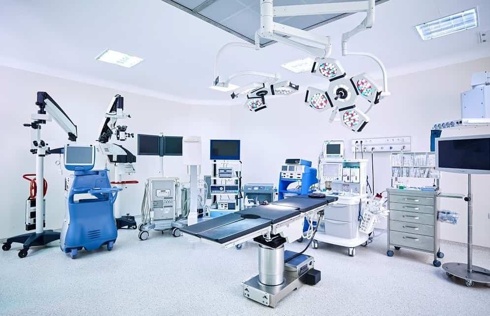
Medical PCBs face stringent design requirements to ensure precision, safety and reliability for life-critical applications. Key considerations include:
- Extremely high reliability and component traceability
- Compatibility with harsh sterilization procedures
- Biocompatible materials compliant with ISO 10993 standards
- Waterproofing for fluid resistance
- Noise reduction for sensor signal clarity
- Radio-transparency for non-interference with imaging equipment
- Radiation hardening for durability under scanning equipment
- High density interconnects facilitating complex component integration
- Flex-rigid construction allowing dynamic movement and embedded placement
Medical PCB advancements focus on greater miniaturization and component density for smaller implantables, higher frequency and data rate capabilities for advanced imaging and robotic surgery, expanding use of flex materials to improve dynamic fit, function and signal integrity, and improved thermal dissipation from higher-powered ICs (Schmartboard, 2021).
Consumer Electronics
The consumer electronics market, which includes products like smartphones, tablets, wearables, home appliances, gaming systems, drones and more, represented a $1 trillion global industry in 2021 (Allied Market Research, 2022). PCBs serve as the “brains” behind these ubiquitous gadgets, although they are also sometimes colloquially referred to as the product’s “heart” or “nervous system.”

While medical PCBs prioritize extreme reliability over costs, consumer electronics take a more cost-driven design approach. Key considerations include:
- High volume manufacturing with low per-unit costs
- Consistent quality despite mass production
- Withstanding everyday abrasion and impact
- Heat and noise reduction for user comfort and safety
- Compact form factors
- Support for continual platform evolution and faster processing speeds
As consumer usage patterns and technological capabilities evolve, PCB innovations focus on supporting integrated components like multi-core processors and advanced GPUs for applications like artificial intelligence (AI), virtual/augmented reality (VR/AR) and Internet of Things (IoT) connectivity. This requires steady PCB platform evolution to support higher frequency signaling, data rates exceeding 25 gigabits per second, complex layered circuitry, intricate thermal management, and growing power demands exceeding 100 watts.
Industrial Equipment
Printed circuit boards are ubiquitous across factory assembly lines and manufacturing facilities. They facilitate process automation, integrate sensors for precision monitoring and analysis, control robotic functions, and regulate power distribution across machinery. The global industrial PC market is projected to grow from $5.4 billion in 2022 to $8.6 billion by 2027, reflecting a 7.9% CAGR (MarketsandMarkets, 2022).

Industrial PCBs must withstand harsh conditions including dust, dirt, moisture, temperature extremes and vibrations. Reliability and safety are paramount if any failures could shut down operations or risk hazardous incidents. Key design considerations reflect these demanding environments:
- Conformal coatings resist contamination from particles, chemicals and liquids
- Durable components withstand shock, impact, drops, and extreme pressure and vibration
- Temperature hardened components function in sub-zero cold or intense furnace heat
- Waterproof enclosures prevent moisture damage
- Thermal management prevents overheating and component burnout
- Backup power solutions prevent shutdowns from power fluctuations
- Remote troubleshooting allows rapid issue identification and remediation
Evolving industrial PCB capabilities focus on wireless interfaces and sensors to reduce cabling and improve flexibility, higher density components to collect and analyze more sensor data, ruggedized constructions to further bolster durability, and improved cooling systems to dissipate intense heat from industrial equipment.
Automotive Applications
Modern vehicles have evolved into sophisticated electronics platforms, with the average car containing over 3,000 individual semiconductors (SEMI, 2022). Electronics facilitate critical functionality for powertrains, safety systems, infotainment, connectivity, comfort and autonomous driving capabilities. The automotive PCB market alone is projected to be valued at $14.5 billion by 2026, up from $10.3 billion in 2019 (Prescient & Strategic Intelligence Private Limited, 2020).

Stringent quality standards and extended product lifecycles shape automotive PCB requirements, which include:
- Extreme temperature durability from -40° to 85°C
- Resistance to humidity, chemicals, vibrations and shocks
- Enhanced signal integrity despite electrical noise
- High voltage capabilities up to 65V
- Low electro-magnetic interference (EMI)
- Failure mode diagnostics and reporting
- Traceability across the supply chain
Key innovations surround integrating more sensors to enhance vehicle autonomy, expanding electronic control units for additional monitored systems, accommodating higher voltage levels, and improving thermal dissipation to enable advanced capabilities without overheating sensitive components (AT&S, 2021).
Aerospace and Avionics
Modern aircraft have highly complex electrical systems that are continuing to expand with the adoption of more fly-by-wire systems and avionics. Fly-by-wire uses electronic interfaces rather than manual controls to manipulate equipment while avionics facilitates electronic communication, navigation and system monitoring capabilities.
The aerospace PCB market was valued at $1.46 billion 2021 and is expected to grow at a 4.5% CAGR from 2022 to 2030 (Grand View Research, 2022). Despite the industry downturn from COVID-19, underlying growth drivers remain strong.

Avionics systems enable modern navigation and communication capabilities while reducing overall aircraft weight. As aerospace PCB applications grow in both scope and complexity, key requirements include:
- Ruggedization for intense vibrations, gravitational forces, drops, crashes, pressure variations
- Shielding against electromagnetic and radio interference
- Low weight to reduce fuel consumption
- Temperature, pressure and altitude durability
- Waterproofing in case of ocean landings
- Flame retardance to resist onboard fires
- High speed signaling for radar and other sensors
- Backup power to support emergency communications
Ongoing innovation surrounds improved thermal dissipation for higher powered applications, reduced signal noise, expanding high-speed data capabilities, integrating more sensors for condition monitoring, and improved shielding against interference.
LED Lighting
Light emitting diodes (LEDs) provide an energy efficient, rapidly responsive and customizable method of illumination well suited for indicators, displays and lighting fixtures. LED lifetimes can exceed 50,000 hours with light output degrading less than 10% over that timeframe (Mousa, 2010). They also turn on/off instantly while achieving full brightness faster than other lighting forms.

When paired with PCBs, LEDs gain enhanced usability and customization. PCBs provide underlying circuitry and connectivity while also serving as a foundational structure and heat sink. Key advantages of PCB-mounted LEDs include:
- Cost effective mass manufacturing
- Customized shapes and sizes
- Integrated control circuitry
- Simple installation onto other PCBs
- Underlying heat dissipation
However, component overheating can severely reduce LED lifetimes and light emission. PCB thermal management is therefore critical, with those offering the best heat dissipation allowing LEDs to achieve 30-70% increased lifecans (Bergquist Company, 2008). Metal-core PCBs (MCPCB) fabricated with insulating dielectric layers mounted onto aluminum or copper substrates provide superior thermal conductivity.
Additional PCB substrates like ceramics and silicon hold opportunities for further enhancements in thermal dissipation, dielectric performance, and integrated sensors and control circuitry. Their high costs currently restrict broad adoption, although pricing could decline with scaling. They represent promising platforms as LED functionality continues advancing in future years through improvements in efficiency, tuning across wider color spectrums, fine-grained color mixing at the pixel level, and potentially onboard data communication capabilities.
Telecommunications Infrastructure
The telecommunications sector relies extensively on PCBs across cellular towers, data centers, network routers and switches, cable network infrastructure, satellite networks, radio communications, and telephone exchanges. The global telecom hardware market was estimated at approximately $100 billion as of 2021 (Statista, 2021).

In addition to high frequency signal integrity and data throughput capabilities, key telecommunications PCB requirements include:
- Ultra high reliability with minimal points of failure
- Rigorous shock and vibration resistance
- Temperature hardened from -40° to 85° C
- Resistant to moisture, dust and corrosion
- EMI/RFI shielding against interference
- High voltage isolation for lightning strikes and AC power
- Extended lifecycles exceeding 15-30 years
- Remote monitoring and diagnostics
Ongoing PCB advancements surround integrating and routing extremely high frequency signaling beyond 600 gigahertz for wireless data transmission, expanding channels for spatial multiplexing, improved antennas and filters for noise reduction and range extension, photonic interfaces for optical data networking, and next-generation architectures for 5G/6G cellular data (5G Americas, 2021).
New Energy
As concerns grow over climate change and fossil fuel dependence, renewable energy sources are expanding around the world. This transition encompasses innovations across solar, wind, geothermal, hydroelectric, hydrogen and nuclear energy. Underpinning these advancements are PCBs enabling more sophisticated power generation, distribution, monitoring and automation capabilities.

The global renewable energy market is expected to grow from $881.7 billion in 2022 to over $2 trillion by 2030, reflecting an 8.4% CAGR (Precedence Research, 2022). This exponential growth will demand PCBs to operate in challenging outdoor environments across all weather conditions over multi-decade lifecycles. Key design focuses include:
- Resilience against moisture, UV radiation, abrasion, lightning and temperature swings from -40° to +85° C
- Hardened power electronics to channel high voltages and currents
- Thermal dissipation for converters, inverters and transformers
- Wireless monitoring interfaces across distributed infrastructure
- Redundancy and remote troubleshooting to minimize downtime
- Long lifecycles exceeding 25 years
Underlying PCB advancements to support next-generation renewable energy implementations include wide bandgap semiconductors able to withstand higher voltages and temperatures, expanding capacity for over 1,500 amps and 1,200 volts, high frequency materials to reduce electromagnetic interference, and flexible substrates allowing streamlined installations, vibration resistance and lightweight portability (Advanced Circuits, 2021).
Semiconductors
Semiconductors underpin virtually every modern electronic device in use today – from home appliances to vehicles, cellular devices to cloud servers. They provide the fundamental on/off electrical switching capabilities enabling all digital electronics functions using solid state, integrated circuit (IC) components.

The global semiconductor market was valued at $595 billion in 2022, an increase of over 20% relative to the previous year reflecting unprecedented demand (Gartner, 2022). PCB advancements help facilitate this rapid innovation across semiconductor fabrication, packaging, testing and integration. Key focus areas include:
- High density interconnects packing ultra-narrow traces and spaces down to 3 micrometers apart
- Low loss, high frequency dielectric materials
- Enhanced signal integrity through controlled impedance interfaces
- Effective thermal dissipation using thermal cladding, thermal vias and metal core PCB substrates
- Customized form factors including rigid, flex and rigid-flex
- Precision alignment and secure mounting techniques
- Rapid prototyping services
Looking ahead, continuing PCB innovations promise to unlock even greater semiconductor functionality, performance and integration density – from heterogenous co-packaged solutions combining computing, memory, optics and more into single integrated packages through to next-generation architectures leveraging advanced interconnects for 2.5/3D stacking. This will facilitate everyday computing devices with expanded intelligence, connectivity and responsiveness powered by ongoing advancements across the supporting PCB ecosystem that makes cutting-edge semiconductor innovation possible.
The path forward for PCB innovation
The path forward for Printed Circuit Board (PCB) innovation is quite dynamic and multifaceted. As electronic applications expand, PCB technology is evolving to meet new challenges and enable novel capabilities. Here’s a look at some of the key aspects of this evolution:
- Diversification of PCB Substrates: Traditionally, PCBs have been made using materials like FR4, but there’s a growing shift towards alternative substrates that offer better performance in specific conditions, such as high temperatures or flexibility.
- Advancements in Conductive Materials: The conductive tracks in PCBs, traditionally made of copper, are seeing innovations in materials to improve conductivity, reduce weight, or enhance durability.
- Innovative Fabrication Techniques: New manufacturing processes are being developed to produce PCBs more efficiently and with greater precision. This includes techniques like additive manufacturing (3D printing) for PCBs.
- Integration of More Complex Components: As electronics get more sophisticated, PCBs are being designed to integrate more complex components, such as microcontrollers, sensors, and RF modules, in smaller spaces.
- Higher Operating Frequencies and Data Transmission Rates: With the rise of applications like 5G and IoT, PCBs are being designed to operate at higher frequencies and support faster data transmission rates.
- Increased Power Outputs and Efficiency: For applications like electric vehicles and renewable energy systems, PCBs need to handle higher power outputs efficiently and safely.
- Extended Lifecycles: There’s a growing emphasis on making PCBs more durable and long-lasting, reducing the need for frequent replacements and thus contributing to sustainability.
- Customization for Specific Industries: Different industries have unique requirements for PCBs. For instance, the medical sector requires highly reliable and precise PCBs, while the automotive industry needs PCBs that can withstand harsh environments.
As technology progresses, these aspects will continue to drive innovation in PCB design and manufacturing, shaping the future of electronics in every sector.
Conclusion
In summary, PCBs form the foundation of electronics across medical equipment, consumer gadgets, industrial machinery, vehicles, airplanes, telecommunication networks and beyond. Their compact and cost-effective design facilitates complex circuit constructions not feasible through individual wiring alone.
And as electronic innovation marches forward, so too will the technology underpinning PCB fabrication and integration. Greater component densities, expanding high-frequency capabilities, improved power transfer and thermal dissipation, more dynamic flexible form factors, and increased miniaturization represent just a subset of the ongoing PCB enhancements still to come. The next wave of technological transformation across industries will ride on the continued evolution of the printed circuit board.

Related Articles
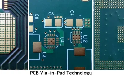
Comprehensive Analysis of PCB Via-in-Pad Technology
Explore the key advantages and challenges of Via-in-Pad technology in PCB design, with expert tips for maximizing performance and reliability.
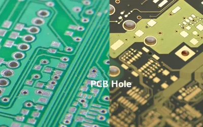
PCB Hole Selection to Optimize PCB Performance and Cost
Discover how to optimize your PCB designs with effective hole selection techniques like back drilling vs buried vias, mechanical vs laser drilling, and HDI stack planning to improve performance while minimizing manufacturing complexity and costs.
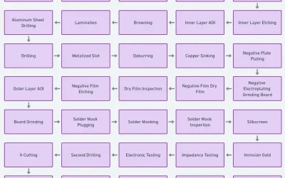
PCB Manufacturing Process Flow – Ultimate Guide Is Here
High-Quality PCB Manufacturing Solutions: Precision, Speed, and Reliability for Your Electronics Projects – From Prototype to Mass Production.