
Back to blog
Comprehensive Guide to PCB Packaging
Ensuring the safe delivery of Printed Circuit Boards (PCBs) is a critical aspect of the manufacturing process. PCBs, integral to most electronic devices today, are delicate and require careful packaging to avoid damage during shipping. This guide delves into the essentials of PCB packaging and shipping.
Benefits of Proper PCB Packaging
Effective PCB packaging is not merely about using the right materials; it plays a crucial role in preventing damage, reducing repair and replacement costs, saving money, maintaining product quality, enhancing customer satisfaction, and complying with industry-specific regulations.
Damage Prevention
Quality packaging protects PCBs from shocks and vibrations during shipping, preventing cracks, bends, or scratches.
Cost Reduction
Minimizing damage rates through proper packaging reduces the need for expensive reworks, repairs, or replacements.
Quality Maintenance
Good packaging safeguards the PCBs, ensuring they maintain their pristine condition, crucial for their performance in the final product.
Customer Satisfaction
Reliable packaging ensures PCBs arrive ready for use, meeting customer expectations.
Regulatory Compliance
Certain industries, like aerospace and defense, have strict packaging regulations that must be adhered to.
Common PCB Packaging Materials
Choosing the right materials is essential to protect PCBs during transport. These materials include cushioning, immobilization, and static protection options.
Cushioning Materials
Options like bubble wrap, foam sheets, air pillows, and paper cushioning provide protection from physical impacts and vibrations. These include bubble wrap, foam sheets, air pillows, and paper cushioning. They are used to protect PCBs from physical impacts and vibrations. Different materials cater to specific needs, such as bubble sizes in bubble wrap for delicate PCBs or anti-static foam for sensitive electronics.
Immobilization Materials
Materials such as cardboard partitions, plastic trays, foam inserts, and specialty tapes prevent PCBs from shifting inside the package.
Static Protection Materials
For static-sensitive PCBs, antistatic bags, foam, metalized bubble wrap, and carbon-loaded plastic are used to prevent static accumulation. These materials prevent PCBs from shifting inside their packaging. Options like cardboard partitions, plastic trays, foam inserts, and specialty tapes are used. Cardboard partitions separate and hold PCBs in place, plastic trays and foam inserts immobilize PCBs by fitting snugly around them, and tapes adhere PCBs to interior packaging surfaces. For static-sensitive PCBs, materials like antistatic bags, foam, metalized bubble wrap, and carbon-loaded plastic are essential. These materials dissipate or prevent static accumulation, protecting PCBs from static discharge that can damage electronic components.
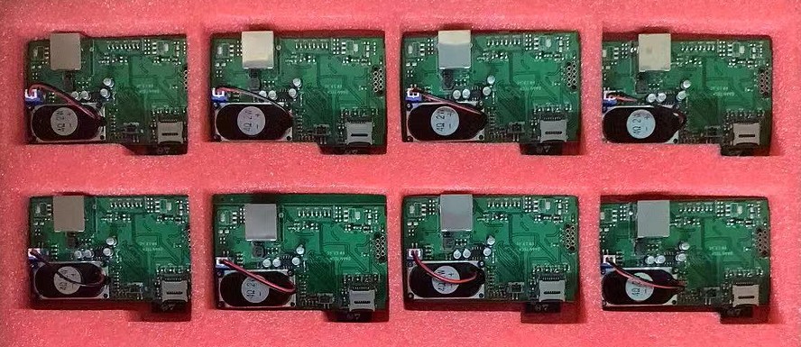
PCB Packaging Methods
A strategic combination of protective materials is used to create a secure package for PCBs. This includes cushion bases, static shielding, immobilization, cushion tops, secure containers, and proper labeling to minimize motion and protect from vibration, shock, and abrasion during shipping.
Cushion Base: The first step involves lining the bottom of the packaging container with cushioning material like bubble wrap, foam, or paper. This base layer absorbs impacts from the bottom.
Static Shielding: For static-sensitive PCBs, this step involves lining the cushioning with a static-dissipating material such as metallized bubble wrap or antistatic foam.
Immobilization: PCBs are then placed inside immobilization materials like die-cut cardboard, plastic trays, or foam cutouts. This step is crucial to prevent shifting and collisions of the PCBs within the packaging.
Cushion Top: A top layer of cushioning is added to protect the PCBs from crushing or dropping impacts.
Secure Container: The PCBs, now safely packaged with multiple protective layers, are placed in a rigid outer container like a box or tube. The container is then securely taped to prevent accidental opening.
Labeling: Proper labeling of the outer container is essential. Labels should indicate that the contents are fragile and include shipping and handling instructions, as well as all necessary shipping labels.
Packing and Labeling Requirements
Standard packing protocols, like using strong outer boxes, cushioning the interior, sealing securely, applying fragile labels, using arrow direction indicators, full address labels, customs paperwork (for international shipments), compliance markings, and center of gravity/lift indicators, are crucial for the safe transport of PCBs.
Preventing Shipping Damage
Despite the best efforts in packaging, certain precautions are necessary to prevent shipping damage. These include using ESD-safe materials, fully immobilizing PCBs, avoiding overpacking, testing for shock/vibration, ensuring proper handling and storage, matching shipping mode to the PCB shipment profile, implementing security measures, and conducting quality reviews.
PCB Packaging Frequently Asked Questions
Addressing common queries about PCB packaging helps clarify best practices and considerations for effective packaging.
ESD Packaging and Large Panel PCBs
Questions like the necessity of antistatic bags, packaging large panel PCBs, labeling identification, the efficacy of ESD packaging, and eco-friendly solutions are commonly addressed.
Conclusion
The success of PCB delivery heavily depends on robust, well-engineered packaging solutions. Matching packaging methods to the unique needs of each PCB shipment, understanding available materials, regulations, transport modes, and potential risks are critical. Effective packaging is a vital component of the overall PCB supply chain. Learn more about Highleap Electronic PCB packaging services.

Recommended Posts
FR408HR PCB Manufacturing Process and Multilayer Reliability
FR408HR multilayer reliability is created by the complete...
KB-6167F PCB Laminate for High-Tg Multilayer PCB Manufacturing
KB-6167F PCB laminate is used when a multilayer PCB needs...
NPG-180BH PCB Material for Automotive and High-Reliability PCB Manufacturing
NPG-180BH PCB material is a Nan Ya halogen-free, high-Tg,...
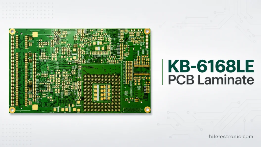
KB-6168LE PCB Laminate for Low Z-CTE Multilayer PCB Manufacturing
KB-6168LE PCB laminate is a Kingboard high-Tg, anti-CAF,...
How to get a quote for PCBs
Let us run DFM/DFA analysis for you and get back to you with a report.
You can upload your files securely through our website.
We require the following information in order to give you a quote:
-
- Gerber, ODB++, or .pcb, spec.
- BOM list if you require assembly
- Quantity
- Turn time
In addition to PCB manufacturing, we offer a comprehensive range of electronic services, including PCB design, PCBA (Printed Circuit Board Assembly), and turnkey solutions. Whether you need help with prototyping, design verification, component sourcing, or mass production, we provide end-to-end support to ensure your project’s success. For PCBA services, please provide your BOM (Bill of Materials) and any specific assembly instructions. We also offer DFM/DFA analysis to optimize your designs for manufacturability and assembly, ensuring a smooth production process.